Figures & data
Figure 1. (a) WVTR values according to the sublayer thickness under 30°C/90% RH. (b) Ca test results of the 30-nm-thick ZAM and Al2O3 films under 30°C/90% and 60°C/90% RH, respectively. AFM images of (c) PET and (d) PET/silamer. (e) Surface roughness and peak-to-valley surface roughness values of the layers deposited on a PET substrate. (f) Normalized conductance curves vs. time of the ZAM, ZAM/silamer, 1.5-dyad ZAM/silamer, and 2.5-dyad ZAM/silamer structures.
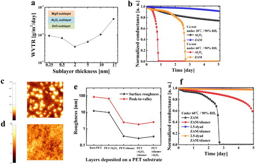
Figure 2. (a) Elemental analysis and (b) cross-sectional TEM images of the 2.5-dyad ZAM/silamer multilayer formed on a Si wafer. (c) Enlarged TEM image of the ZAM NL film (inset: enlarged TEM images of the ZAM NL films in scale).
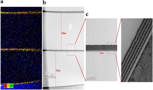
Figure 3. (a) Elastic modulus and hardness values of the Al2O3, ZAM, and silamer layers (inset: elastic modulus and hardness values of silamer). (b) Changes in the WVTR values of the 2.5-dyad ZAM/silamer and 2.5-dyad Al2O3/silamer multilayers before and after the bending tests with 0.63% bending strain. (c) WVTR values of the 2.5-dyad ZAM/silamer multilayer after the bending tests as a function of the bending strain (0% strain means the unbent multilayer).
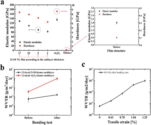
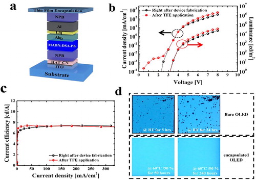
Figure 4. (a) Schematic structure of blue-emitting FOLEDs. (b) J–V–L characteristics of FOLEDs before and after TFE to OLEDs. (c) Current efficiency vs. current density. (d) Cell images of bare and encapsulated OLEDs under 60°C/90% conditions.