
Figures & data
Table 1. Detailed deposition parameters for each layer of ECD.
Figure 1. Evolution in the SEM and AFM surface morphologies of the Ag film deposited on the ITO/Si substrate as a function of Ag deposition time (tdep): tdep = (a)–(e) 13 s, (b)–(f) 15 s, (c)–(g) 17 s and (d)–(h) 19 s.
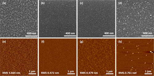
Figure 2. Variations in XRD patterns of IAI films inserted with Ag films of varying thickness.
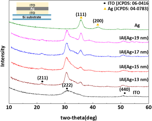
Figure 3. (a) Resistivity, carrier concentration of the IAI multilayers as a function of Ag thickness. (b) Optical transmittance spectra of the IAI multilayers as a function of Ag thickness. (c) Figure of merit and sheet resistance of the IAI multi-layer structures as a function of Ag thickness.
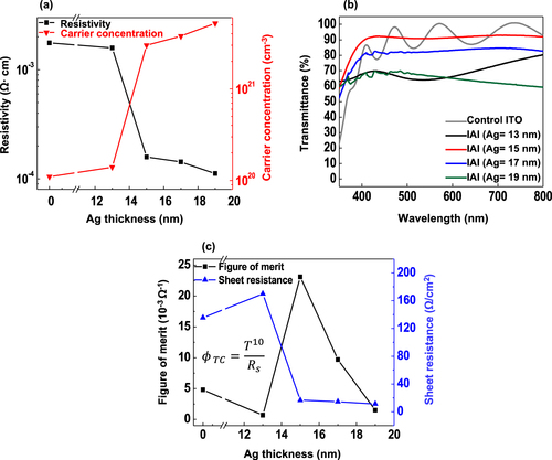
Table 2. The sheet resistance, optical transmittance, and the figure of merit of the IAI multilayers with Ag deposition time varying from 0 s to 19 s.
Figure 4. CV characteristics of the ECDs with (a) single ITO and (b) IAI-15 s bottom electrodes. The 5th cycle test result was inserted, and the scan rate during the CV measurements was 50 mV/s. (c) Optical transmittance spectra of ECDs with single and IAI-15 s bottom electrodes in the colored and bleached states under sweep voltages of ±1.0 V after 5 cycle loadings. (d) CA characteristics of both ECDs under a sweep voltage of ±1.0 V after 5 cycle loadings. The negative and positive currents represent the coloring and bleaching process, respectively.
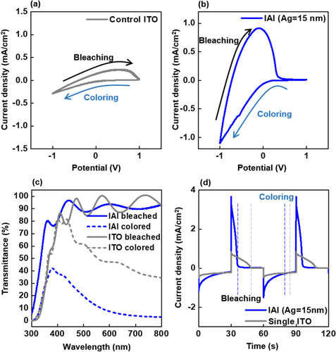
Figure 5. Plan-view and cross-sectional SEM images for the WO3 films prepared at different sputtering pressures: (a)–(d) 1.0 Pa, (b)–(e) 1.5 Pa and (c)–(f) 2.0 Pa.
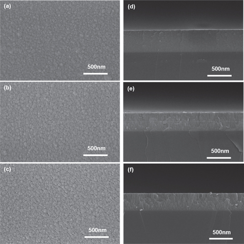
Figure 6. Measured XRR data for the WO3 films on the SiO2/Si substrate under different Pchamber conditions of 1.0, 1.5 and 2.0 Pa. Inset shows an enlarged graph of the XRR spectra.
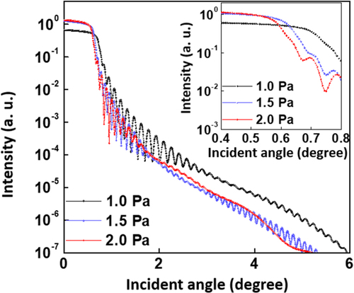
Figure 7. XPS spectra of W 4f for the films deposited at (a) 1.0 Pa, (b) 1.5 Pa, (c) 2.0 Pa, and (d) the O/W ratio as a function of sputtering pressure.
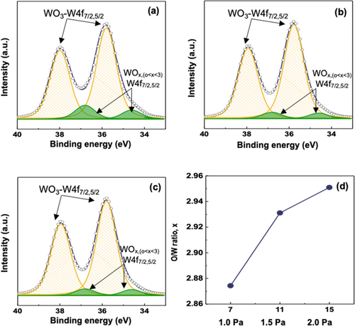
Figure 8. (a)–(c) Cyclic voltammograms and (d)–(f) corresponding results on optical transmittance results.
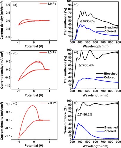
Figure 9. (a) Variation in the optical density difference (ΔODλ) with respect to the wavelength. (b) Coloration efficiency of WO3 films at different P chamber conditions of 1.0, 1.5 and 2.0 Pa. (c) The current density corresponding to the process of the response time.
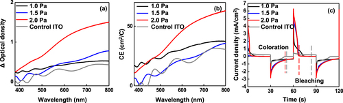
Table 3. Device performance comparisons of ECDs with WO3-based EC materials.