Figures & data
Figure 1. (a) Optical transmittance of ZnON film. The inset graph shows the extracted optical band gap. (b) AFM image of ZnON with a scan size of 5 × 5 um.
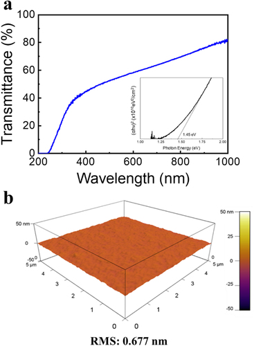
Figure 2. (a) Transfer and (b) Output curves of the proposed ZnON TFTs.
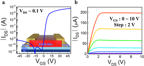
Figure 3. (a) A 3D layout of the proposed sputtering process for uniform Te-film deposition at low temperature in the presence of Ar gas flow. (b) Thickness profiles of the proposed Te-film in terms of AFM image (upside) and height profile (downside). (c) Raman spectroscopy of the deposited Te-film with an inset of Te-substrate and marking of Raman measurement point.
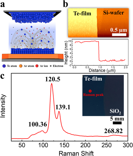
Figure 4. (a) Transfer curve of the fabricated Te-based TFT along with a schematic and real image of the TFT. (b) Output curve of the proposed Te-based TFT at VGS ranges from 10 V to −50 V with a step of −10 V.
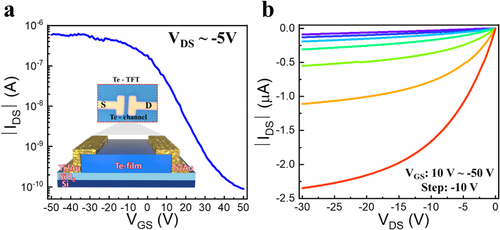
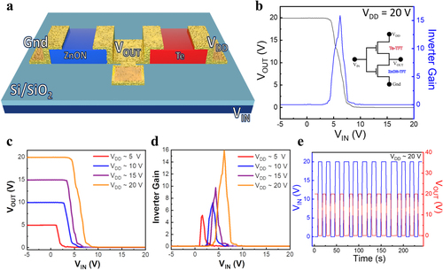
Figure 5. (a) A schematic layout of the hybrid Te and ZnON TFTs-based CMOS inverter device. (b) Transfer voltage and inverter gain curves of the proposed inverter device at VDD of 20 V with an inset of the schematic circuit layout. (c) and (d) Transfer voltage and inverter gain curves of the inverter device at different VDD range from 5 to 20 V with a step of 5 V. (e) Time-domain output curve measurements of the inverter device by applying VIN pulse of 20 V at VDD 20 V.