Figures & data
Figure 1. Schematic diagram of the proposed AS-ALD method using inkjet-printed ALD-inhibition test patterns and lift-off process.
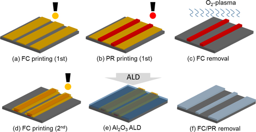
Figure 2. PR dot patterns inkjet-printed with a single drop on hydrophilic tracks: (a) Wtrack = 60 µm, (b) Wtrack = 50 µm, (c) Wtrack = 40 µm, (d) Wtrack = 30 µm (Wtrack = hydrophilic track width between FC line patterns).
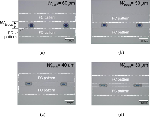
Figure 3. Inkjet-printed PR line patterns on hydrophilic tracks (Wtrack): (a) Wtrack = 60 µm; (b) Wtrack = 50 µm; (c) Wtrack = 40 µm; (d) Wtrack = 30 µm; (e) cross-sectional profile (Wtrack = a hydrophilic track width between FC line patterns).
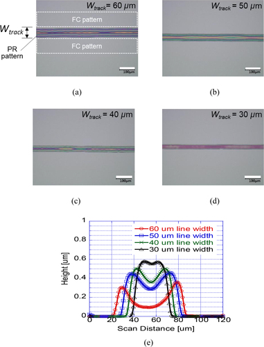
Table 1. Ink-jetting performance for mixing ratios of PR and EL solvents.
Figure 4. PR patterns overprinted on hydrophilic tracks using layer–by–layer printing method: (a) optical microscopic image of 3-times printed PR pattern, (b) cross-sectional profile of 30 μm line width, (c) cross-section profile of 60 μm line width, (d) optical microscopic image of FC/PR pattern.
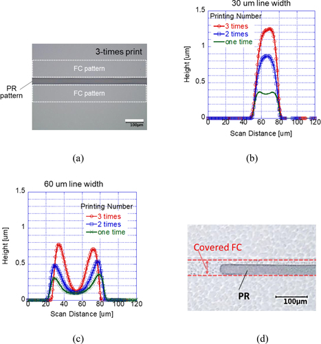
Figure 5. Results of AFM analysis on 1 μm × 1 μm scanned area before and after Al2O3 ALD on various surfaces: (a) bare Si; (b) Al2O3-deposited Si surface; (c) FC-coated Si (FC/Si) surface; (d) Al2O3-deposited FC/Si surface; (e) PR-coated Si (PR/Si) surface; (f) Al2O3-deposited PR/Si surface; (g) FC-covered PR/Si (FC/PR/Si) surface; (h) Al2O3-deposited FC/PR/Si surface.
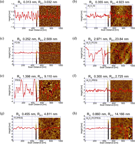
Figure 6. Results of AFM and TOF-SIMS analyses of Al2O3 AS-ALD process using FC inhibition pattern: (a) AFM image of FC inhibition pattern on Si substrate; (b) AFM image of Al2O3 pattern formed by O2 plasma lift-off process; (c) TOF-SIMS AlO– signal of FC patterns on Si substrate, (d) TOF-SIMS CF- signal of FC patterns on Si substrate, (e) TOF-SIMS AlO– signal after Al2O3 deposition, (f) TOF-SIMS depth intensity of AlO– signal in the background and FC pattern regions.
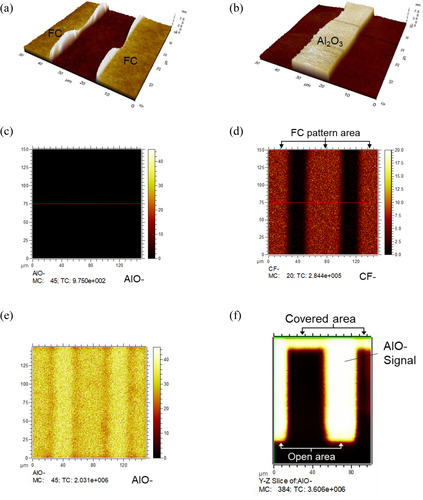
Figure 7. Optical microscope images before and after ultrasonic agitation using acetone for Al2O3-deposited PR pattern: (a) Al2O3 deposited PR patterns; (b) Al2O3-deposited PR pattern after 15-min ultrasonic agitation.
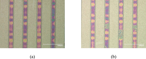
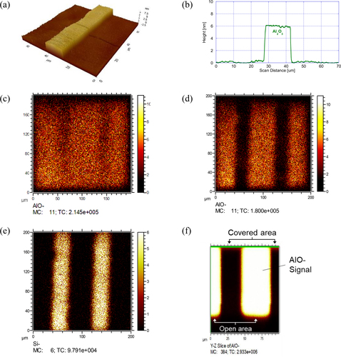
Figure 8. Results of AFM and TOF-SIMS analyses of Al2O3 AS-ALD process using FC/PR inhibition pattern: (a) three-dimensional image and (b) cross-sectional profile of patterned Al2O3 measured by AFM; (c) TOF-SIMS AlO– signal after lift-off process using 0.45 µm thick FC/PR pattern; (d) TOF-SIMS AlO- signal and (e) Si– signal after lift-off process using 1.28 µm thick FC/PR pattern; (f) TOF-SIMS depth intensity of AlO– signal in the background and 1.28 µm thick FC/PR pattern regions.