
Figures & data
Figure 1. Proposed HA grating cell. (a) Operating schematic of the proposed HA grating cell. (b) Top view of LC director configurations. Calculated LC director distributions and phase difference profiles in (c) x, (d) y, and (e) diagonal directions.
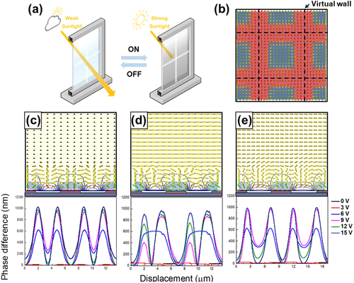
Figure 2. Calculated (a) voltage-dependent diffraction efficiency and (b) condition for each diffraction order. (c) Polarized optical microscopy (POM) images of the proposed device with crossed polarizers and full-wave plate. (d) Diffraction pattern of the proposed device at different applied voltages from 0 to 12 V.
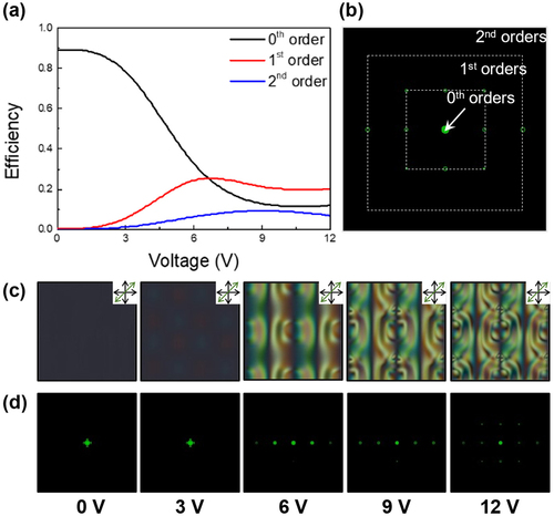
Figure 3. (a) Haze values of the proposed device and (b) calculated transparent and opaque state images with the Kangwon National University (KNU) logo from 0 to 15 V.
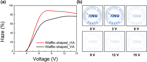
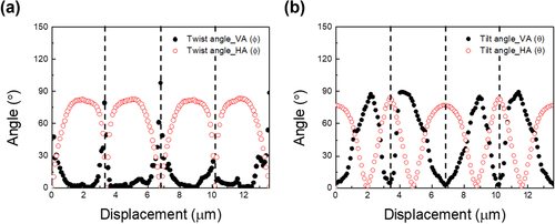
Figure 4. Calculated angles of HA and VA grating cells at 15 V. (a) Twist and (b) tilt angles (vertical dotted lines represent the position of the virtual wall).
Supplemental Material
Download MS Word (150.9 KB)Data availability
Data underlying the results presented in this paper are not publicly available at this time but may be obtained from the authors upon reasonable request.