Figures & data
Figure 1. (a) UV-visible spectrum of the as-prepared WSe2 solution. The inset shows the photograph of each dispersion in isopropanol. (b) Raman spectra of WSe2. The inset shows the atomic displacement of the E2g1 and A1g Raman-active modes. (c) AFM image of the exfoliated WSe2 nanoflakes and the corresponding height profile (scale bar: 500 nm). (d) High-resolution TEM image of the exfoliated WSe2 nanoflakes. The inset shows the selected-area electron diffraction image (scale bar: 2 nm).
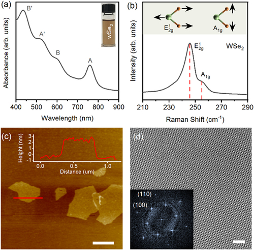
Figure 2. (a) Schematic of transistor fabrication by drop-casting with the 2D ink. (b) Optical micrograph of the as-fabricated WSe2 transistor (scale bar: 100 µm). (c) Cross-sectional TEM image of the WSe2 thin film on the Si/SiO2 substrate (scale bar: 20 nm).
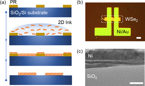
Figure 3. (a) IDS–VGS transfer curves at VDS = −1 V for the pristine and FeCl3-doped WSe2 (60 µg/mL) TFTs on a SiO2/Si substrate with a 100 nm-thick SiO2 layer. VDS is −1 V. The width and length of the channel are 725 and 50 µm, respectively. (b) Output curve of the corresponding FeCl3-doped WSe2 TFT. (c) UPS spectra showing the secondary electron cut-off and (d) valence band of pristine and FeCl3-doped WSe2 thin films (60 µg/mL). (e) Schematic energy diagram of the Ni/Au and WSe2 contacts before and after doping. (f) Schematic energy diagram at the interface between the nanoflakes in the channel with a bias voltage applied after doping.
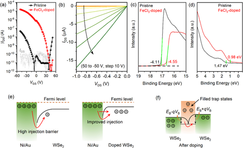
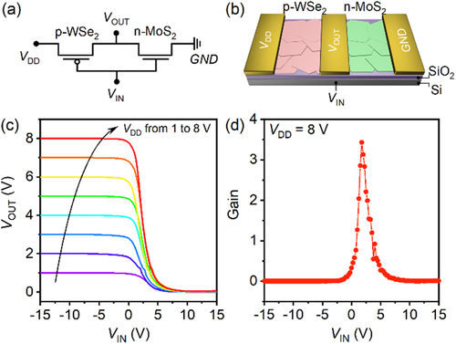
Figure 4. Solution-processed complementary metal-oxide-semiconductor (CMOS) inverter. (a) Circuit diagram of the CMOS inverter. (b) Schematic of a CMOS inverter with p-WSe2 and n-MoS2 channels. (c) Voltage transfer characteristics of the CMOS inverter as a function of the input voltage with different VDD values from 1 to 8 V. The FeCl3-doping concentration for p-WSe2 is 60 µg/mL. (d) Corresponding gains of the inverter from c at VDD = 8 V.