Figures & data
Scheme 1. The schematic illustration of the chemical transformation of Cs4PbBr6 into CsPbBr3 nanorods due to ligand-regulated reactions at the water-oil interface. The bottom is the images of Cs4PbBr6 NCs to the intermediate stage (oil-water ligand modulation) to CsPbBr3 nanorods.
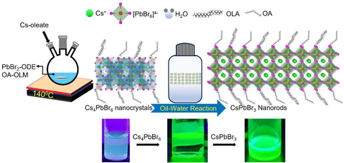
Figure 1. (a) Field-emission transmission electron microscope (FE-TEM) image, (b-c) the histogram of the average length and width of the CsPbBr3 nanorod for 44 h of ligand-modification times, (d) FE-TEM image, (e-f) the histogram of the average length and width of the nanorods for 33 h of ligand modification times, (g) FE-TEM image, and (h-i) the histogram of the average length and width of the nanorod for 22 h of ligand modification times.
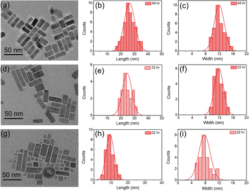
Figure 2. (a) XRD pattern of nanopolyhedrons Cs4PbBr6 NCs and CsPbBr3 nanorods (mixed phase and final nanorods). Enlarged XRD pattern of (b) (100) crystal plane, (c) (110) crystal plane, (d) (200) crystal plane, (e) (210) crystal plane, and (f) (211) crystal plane of Cs4PbBr6 NCs and CsPbBr3 nanorods (mixed phase and final nanorods). (g) PLQY as a function of different ligand-modification times (0, 11, 22, 33, 44, and 55 hr), and (h) the absorption and photoluminescent (PL) spectra of CsPbBr3 nanorods (44 hr).
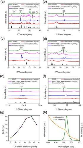
Figure 3. (a) XPS spectra of CsPbBr3 nanorods film. High-resolution XPS spectra of (b) Cs 3d, (c) Pb 4f, and (d) Br 3d of nanorods.
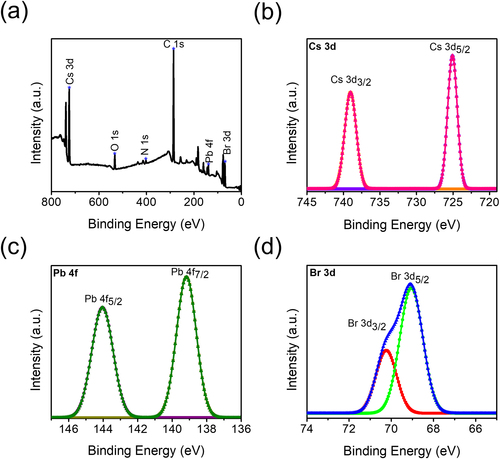
Figure 4. (a) Angle-dependent photoluminescence intensity of the nanorods, where isotropic (red) and perfect horizontal (blue) orientation cases are added for comparison; and (b) refractive index (n) and extinction coefficient (k) of the thin film of anisotropic nanorods
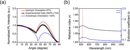
Figure 5. (a) The energy level diagram of functional layers in PeLEDs, (b-c) schematic illustration and cross-sectional TEM images of PeLEDs, (d) current density-voltage-luminance characteristics, (e) external quantum efficiency vs. current density curve, (f-g) histogram of maximum external quantum efficiency and luminance values. (h-i) current efficiency-power efficiency vs. current density, and EL spectra of ANR-LEDs. The inset of Figure (i) is the operation image of the LED under 4.8 V.
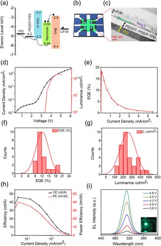
Table 1. Comparison of optoelectronic properties of PeLEDs based on CsPbBr3.
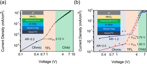
Figure 6. The logarithm current density vs. voltage curves of single-carrier devices for (a) aspect ratio (AR) of 2.2 and (b) of 2.0 and 1.2, respectively. The insets are schematic illustrations of the hole-only devices.