Figures & data
Figure 1. The structures of single-unit (top) and tandem (bottom) devices. The inset photo is the fabricated tandem OLED.
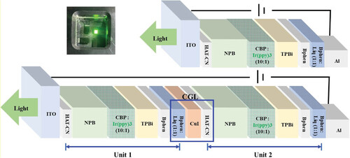
Figure 2. (a) XRD patterns and (b) UV–Vis transmittance spectra of thermally evaporated CuI film deposited on a glass substrate.
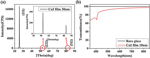
Figure 3. (a) UPS graph and (b) Tauc plot of Bphen:Liq, (c) schematic band diagram of the tandem device.

Figure 4. (a) Band diagram of devices prepared with and without CuI, (b) corresponding plot of current density versus voltage and comparison of I–V performance between Device 2 and Device 1.
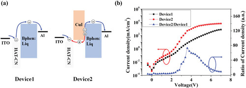
Figure 5. (a) Band diagram of CGL devices with double insulation layers prepared with and without CuI (Devices 3 and 4, respectively). (b) Capacitance versus voltage (C-V) plots of Device 3 and Device 4.
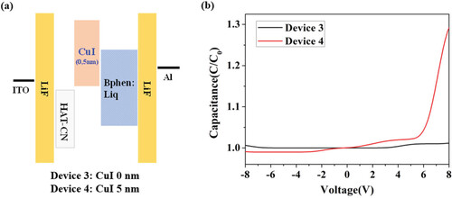
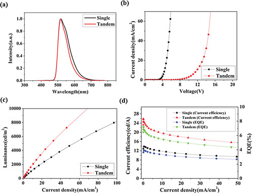
Figure 6. (a) Normalized EL spectrum of single and tandem devices, (b) Current density versus applied voltage (c) Luminance versus current density, (d) Current efficiency (left side) and EQE (right side) versus current density of single unit and tandem devices.