
Figures & data
Table 1. Physical properties of LC mixtures for TV applications.
Table 2. Physical properties of LC mixtures for fast response time.
Figure 1. Structures of high-end TFT-LCDs with local dimming mini-LEDs and QD films. (a) a homogeneously aligned FFS LC cell with no compensation film, and (b) a thin film containing dichroic dyes on top of a conventional polarizer. Macroscopic photographs comparing dark states surrounding a bright circle image when the dichroic film formed between two glass substrates exists above an uncompensated TV panel for (c) 1 wt% and (d) 2 wt% dye-doped films. Case (d) demonstrates excellent dark states surrounding the bright circle image in all viewing directions [Citation30].
![Figure 1. Structures of high-end TFT-LCDs with local dimming mini-LEDs and QD films. (a) a homogeneously aligned FFS LC cell with no compensation film, and (b) a thin film containing dichroic dyes on top of a conventional polarizer. Macroscopic photographs comparing dark states surrounding a bright circle image when the dichroic film formed between two glass substrates exists above an uncompensated TV panel for (c) 1 wt% and (d) 2 wt% dye-doped films. Case (d) demonstrates excellent dark states surrounding the bright circle image in all viewing directions [Citation30].](/cms/asset/75a1eaf5-5328-4894-bb9a-0efb7b670b28/tjid_a_2281224_f0001_oc.jpg)
Figure 2. LC molecular responses under different field frequencies (e.g. 60 Hz [left] and 1 Hz [right]). At 1 Hz, geometrical deformation can occur having flexoelectric polarization.
![Figure 2. LC molecular responses under different field frequencies (e.g. 60 Hz [left] and 1 Hz [right]). At 1 Hz, geometrical deformation can occur having flexoelectric polarization.](/cms/asset/2211a743-f9cd-42bb-a56e-5df8fc7e2b28/tjid_a_2281224_f0002_oc.jpg)
Figure 3. Brightness difference between frames based on flexoelectric effect in an FFS electrode structure [Citation42].
![Figure 3. Brightness difference between frames based on flexoelectric effect in an FFS electrode structure [Citation42].](/cms/asset/d0871526-b3a3-4e7c-904e-e30acabec5f7/tjid_a_2281224_f0003_oc.jpg)
Figure 4. Structural difference and comparison between FFS and IPS modes in which flexoelectric effect exists at low-frequency driving [Citation42].
![Figure 4. Structural difference and comparison between FFS and IPS modes in which flexoelectric effect exists at low-frequency driving [Citation42].](/cms/asset/3ee817b6-778d-42e2-8ce6-36f2a5a00f05/tjid_a_2281224_f0004_oc.jpg)
Figure 5. Flexoelectric polarization of pear and banana-shaped molecules and the contribution of dipoles of -LC (bend) and quadrupoles (splay) to flexoelectric coefficients.
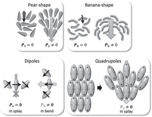
Figure 6. Schematic comparison of pixel structures and simulated transmittance between AFFS and HFFS modes [Citation47].
![Figure 6. Schematic comparison of pixel structures and simulated transmittance between AFFS and HFFS modes [Citation47].](/cms/asset/0ab69603-084a-4806-a435-559efa6ddc5d/tjid_a_2281224_f0006_oc.jpg)
Figure 7. Comparison of voltage-dependent transmittance curves in high-resolution mobile TFT-LCDs. The HFFS mode shows much-improved transmittance, as also shown in the microscopic image of a pixel [Citation47].
![Figure 7. Comparison of voltage-dependent transmittance curves in high-resolution mobile TFT-LCDs. The HFFS mode shows much-improved transmittance, as also shown in the microscopic image of a pixel [Citation47].](/cms/asset/b8dd661c-8b44-42a2-aced-2a116c33f7eb/tjid_a_2281224_f0007_oc.jpg)
Figure 8. Comparison of pixel structures between (a) IPS-Pro pixel and (b) IPS-Pro Next pixel [Citation48,Citation49].
![Figure 8. Comparison of pixel structures between (a) IPS-Pro pixel and (b) IPS-Pro Next pixel [Citation48,Citation49].](/cms/asset/d40eaddd-42e4-44ee-9020-87eb95cf885d/tjid_a_2281224_f0008_oc.jpg)
Figure 9. Comparison of pixels of 47′′ IPS-LCDs [Citation48].
![Figure 9. Comparison of pixels of 47′′ IPS-LCDs [Citation48].](/cms/asset/0191119d-892d-46a8-9ede-f7c343b65ee4/tjid_a_2281224_f0009_oc.jpg)
Figure 10. Cross-sectional view of a pixel structure of BOE’s high transmittance ADS mode along data and gate line. The thickness of an organic (ORG) layer is controlled by a full-tone (FT) and half-tone (HT) mask [Citation50].
![Figure 10. Cross-sectional view of a pixel structure of BOE’s high transmittance ADS mode along data and gate line. The thickness of an organic (ORG) layer is controlled by a full-tone (FT) and half-tone (HT) mask [Citation50].](/cms/asset/d4e09915-a590-41b9-b5e8-299cadfd208d/tjid_a_2281224_f0010_oc.jpg)
Figure 11. Evolution of process routes from ADS to i-ADS and high transmittance ADS (HADS) utilizing ORG layer. ADS requires two ITO layers and 1ITO and 2ITO represent first and second layers, respectively [Citation12].
![Figure 11. Evolution of process routes from ADS to i-ADS and high transmittance ADS (HADS) utilizing ORG layer. ADS requires two ITO layers and 1ITO and 2ITO represent first and second layers, respectively [Citation12].](/cms/asset/f0b6e097-d3fd-45e1-b1b6-2a25b7e302f5/tjid_a_2281224_f0011_oc.jpg)
Figure 12. Typical structure of SA-VA additive (e.g. Compound 5) and SA-VA process. After LC filling, the polar (blackhead groups) interact with the substrates and give a vertical orientation. Under the application of a voltage and irradiation by UV light, the tilt is formed and fixed. The RMs polymerize to form a film at the substrate surfaces [Citation57].
![Figure 12. Typical structure of SA-VA additive (e.g. Compound 5) and SA-VA process. After LC filling, the polar (blackhead groups) interact with the substrates and give a vertical orientation. Under the application of a voltage and irradiation by UV light, the tilt is formed and fixed. The RMs polymerize to form a film at the substrate surfaces [Citation57].](/cms/asset/077ea3b3-354a-45f1-b0fd-29d3d5e0a228/tjid_a_2281224_f0012_oc.jpg)
Figure 13. Schematic illustration of the fabrication process for the self-alignment FFS-mode LC cell (Self-FFS cell): (a) before preparing the SAL and (b) after preparing the SAL and obtaining the homogeneous alignment, (c) the material design concept of the additive agents, and (d) the monomer-carrying chalcone unit used in this study [Citation59,Citation60].
![Figure 13. Schematic illustration of the fabrication process for the self-alignment FFS-mode LC cell (Self-FFS cell): (a) before preparing the SAL and (b) after preparing the SAL and obtaining the homogeneous alignment, (c) the material design concept of the additive agents, and (d) the monomer-carrying chalcone unit used in this study [Citation59,Citation60].](/cms/asset/8fc1b1e8-71ca-46db-8f54-3c4265857e21/tjid_a_2281224_f0013_oc.jpg)
Figure 14. Simulated transmittance in a pixel of PS-VA mode: (a) Fishbone electrode (pixel) and plane electrode (common), (b) Transmittance profile in different resolution, and comparison of transmittance with LC orientation profile in (c) PS-VA and (d) C-PS-VA mode [Citation65].
![Figure 14. Simulated transmittance in a pixel of PS-VA mode: (a) Fishbone electrode (pixel) and plane electrode (common), (b) Transmittance profile in different resolution, and comparison of transmittance with LC orientation profile in (c) PS-VA and (d) C-PS-VA mode [Citation65].](/cms/asset/8be878d6-e6bd-4eb4-8489-370107de64e8/tjid_a_2281224_f0014_oc.jpg)
Figure 15. (a) Structure of wide-viewing-angle film with representative three optical rays and (b) Comparison of iso-luminance contours [Citation68]. AG indicates anti-glare film.
![Figure 15. (a) Structure of wide-viewing-angle film with representative three optical rays and (b) Comparison of iso-luminance contours [Citation68]. AG indicates anti-glare film.](/cms/asset/9eb31c02-b1aa-4699-baf4-f036b0ffade4/tjid_a_2281224_f0015_oc.jpg)
Figure 16. Structure of blue phase I [Citation72].
![Figure 16. Structure of blue phase I [Citation72].](/cms/asset/4bd6198f-295b-4a91-9b86-9fd005ae5b92/tjid_a_2281224_f0016_oc.jpg)
Figure 17. Structure of blue phase III [Citation72]
![Figure 17. Structure of blue phase III [Citation72]](/cms/asset/1906ea6f-f317-47d9-8af9-1d1f328fafe7/tjid_a_2281224_f0017_oc.jpg)
Table 3. Normal mode and blue phase mode [Citation72–74].
Figure 18. Polymer-stabilized blue phase I and its world’s prototype were made by Samsung Electronics in the exhibition of the SID 2008 [Citation75,Citation76].
![Figure 18. Polymer-stabilized blue phase I and its world’s prototype were made by Samsung Electronics in the exhibition of the SID 2008 [Citation75,Citation76].](/cms/asset/08104f72-6b47-4af4-b5b5-d0b199393a5d/tjid_a_2281224_f0018_oc.jpg)
Figure 19. Comparison of polymer-stabilized BPI, isotropic phase, and BPI and the switching property of BPIII [Citation72,Citation73].
![Figure 19. Comparison of polymer-stabilized BPI, isotropic phase, and BPI and the switching property of BPIII [Citation72,Citation73].](/cms/asset/ce94ebcf-c6ce-4046-804f-d26702ef02a4/tjid_a_2281224_f0019_oc.jpg)
Figure 20. BP color tuneable Photonic soft crystals [Citation84].
![Figure 20. BP color tuneable Photonic soft crystals [Citation84].](/cms/asset/de7ef6d8-bd21-4edc-988c-8395a6930073/tjid_a_2281224_f0020_oc.jpg)
Figure 21. Molecular structures and modification of ferroelectric LCs in nematic phase [Citation87,Citation103].
![Figure 21. Molecular structures and modification of ferroelectric LCs in nematic phase [Citation87,Citation103].](/cms/asset/bbec628e-b2e9-4d88-a1a9-64ba29b192a8/tjid_a_2281224_f0021_oc.jpg)