
Figures & data
Figure 1. Schematic diagram of the cross-sectional view model of (a) backlit (b) emissive displays (Figures reproduced with permission from [Citation4] Copyright © 2019, John Wiley and Sons) and (c) band–gap energy versus lattice constants profile of III–nitrides (Al, In, Ga)-N (inside the dashed lines denotes that lattice-matched points of InxGa1−xN/InyAl1−yN that corresponds to blue, green and red emission wavelength, respectively). Adopted from Ref. [Citation29]. Reproduced under the terms of an open-access Creative Commons CC BY 4.0 license.
![Figure 1. Schematic diagram of the cross-sectional view model of (a) backlit (b) emissive displays (Figures reproduced with permission from [Citation4] Copyright © 2019, John Wiley and Sons) and (c) band–gap energy versus lattice constants profile of III–nitrides (Al, In, Ga)-N (inside the dashed lines denotes that lattice-matched points of InxGa1−xN/InyAl1−yN that corresponds to blue, green and red emission wavelength, respectively). Adopted from Ref. [Citation29]. Reproduced under the terms of an open-access Creative Commons CC BY 4.0 license.](/cms/asset/c0d01663-77b1-4619-abc5-6e133c491c90/tjid_a_2282937_f0001_oc.jpg)
Table 1. Performance matrix of LCD, OLED, and µ-LED systems [Citation14].
Figure 2. STEM-HAAF images illustrating the side wall appearance of InGaN MQW with different fabrication techniques: (a) dry etch, (b) wet etch, (c) sol–gel SiO2 deposition, and plasma-enhanced ALD SiO2 deposition of thicknesses measuring (d) 2 nm and (e) 60 nm. Figures reproduced with permission from [Citation84]. Copyright © 2022.
![Figure 2. STEM-HAAF images illustrating the side wall appearance of InGaN MQW with different fabrication techniques: (a) dry etch, (b) wet etch, (c) sol–gel SiO2 deposition, and plasma-enhanced ALD SiO2 deposition of thicknesses measuring (d) 2 nm and (e) 60 nm. Figures reproduced with permission from [Citation84]. Copyright © 2022.](/cms/asset/d243807b-26cb-4b87-9ef7-b0af322084a7/tjid_a_2282937_f0002_oc.jpg)
Figure 3. Schematic representation of VLS metal catalyst assisted III-nitride NW growth sequence process.
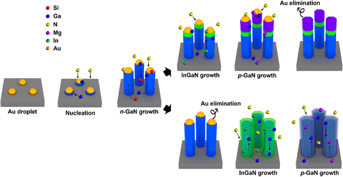
Figure 4. SEM images of (a) N-rich and (b) Ga-rich flux conditions, respectively. Figures reprinted with permission from Ref. [Citation116], Copyright © 2016, Elsevier.
![Figure 4. SEM images of (a) N-rich and (b) Ga-rich flux conditions, respectively. Figures reprinted with permission from Ref. [Citation116], Copyright © 2016, Elsevier.](/cms/asset/f44d5f37-b69c-4dbf-9a4b-9f0da34a40e3/tjid_a_2282937_f0004_ob.jpg)
Figure 5. Tilt-view FE-SEM images of GaN NWs grown on Au-Si (111) at growth temperatures of (a) 800, (b) 850, (c) 900, (d) 950, and (e) 1000 °C. Figures reprinted with permission from Ref. [Citation117], Copyright © 2016, IOP Publishing, Ltd.
![Figure 5. Tilt-view FE-SEM images of GaN NWs grown on Au-Si (111) at growth temperatures of (a) 800, (b) 850, (c) 900, (d) 950, and (e) 1000 °C. Figures reprinted with permission from Ref. [Citation117], Copyright © 2016, IOP Publishing, Ltd.](/cms/asset/e9d16fee-7d10-4a7f-8089-9a5f7a128ca3/tjid_a_2282937_f0005_ob.jpg)
Figure 6. FE-SEM characteristic images GaN NWs (a) AlN buffer layer thickness 60 nm, (wire density 5 numbers/mm2) (b) AlN buffer layer thickness 80 nm–100 nm, (wire density 160 numbers/mm2). Figures reproduced with permission from Ref. [Citation33], Copyright © 2016, Elsevier.
![Figure 6. FE-SEM characteristic images GaN NWs (a) AlN buffer layer thickness 60 nm, (wire density 5 numbers/mm2) (b) AlN buffer layer thickness 80 nm–100 nm, (wire density 160 numbers/mm2). Figures reproduced with permission from Ref. [Citation33], Copyright © 2016, Elsevier.](/cms/asset/b68c485b-e9fd-4504-9f28-879a4a3cf306/tjid_a_2282937_f0006_ob.jpg)
Figure 7. The typical nucleation approach. Smaller islands could face extinction as Ga diffuses toward other stable nuclei. (b) Illustration of the production of nanocolumns from stable nuclei revealing the direct integration of impinging Ga flux (j(L)) and substrate Ga diffusion (j(D)) into the nucleation base of the building block, extending to its apex. By multiplying the average diffusion length of Ga adatoms by two, the average distance between nanocolumns is calculated, where dCR denoted that the average critical distance signifies the typical proximity from which Ga adatoms can access the base of the nanocolumn. This distance is notably influenced by the growth temperature. Figures reproduced with permission from Ref. [Citation118] Copyright © 2008, Elsevier.
![Figure 7. The typical nucleation approach. Smaller islands could face extinction as Ga diffuses toward other stable nuclei. (b) Illustration of the production of nanocolumns from stable nuclei revealing the direct integration of impinging Ga flux (j(L)) and substrate Ga diffusion (j(D)) into the nucleation base of the building block, extending to its apex. By multiplying the average diffusion length of Ga adatoms by two, the average distance between nanocolumns is calculated, where dCR denoted that the average critical distance signifies the typical proximity from which Ga adatoms can access the base of the nanocolumn. This distance is notably influenced by the growth temperature. Figures reproduced with permission from Ref. [Citation118] Copyright © 2008, Elsevier.](/cms/asset/abc0e575-aafe-44d9-a807-029728ed29de/tjid_a_2282937_f0007_oc.jpg)
Figure 8. SEM comparison of GaN NWs, (a) with rotation (20 rpm) and (b) without rotation, using MBE. Figures reproduced with permission from Ref. [Citation42], Copyright © 2009, Elsevier.
![Figure 8. SEM comparison of GaN NWs, (a) with rotation (20 rpm) and (b) without rotation, using MBE. Figures reproduced with permission from Ref. [Citation42], Copyright © 2009, Elsevier.](/cms/asset/ef37eb0b-aa40-4e87-9ac5-f3c502177d6f/tjid_a_2282937_f0008_ob.jpg)
Figure 9. Schematic illustration of SAG growth mechanism. Figures reproduced with permission from Ref. [Citation128], Copyright © 2009, Elsevier.
![Figure 9. Schematic illustration of SAG growth mechanism. Figures reproduced with permission from Ref. [Citation128], Copyright © 2009, Elsevier.](/cms/asset/8f1eeaae-3a75-4e85-a1d6-a171627cc2c0/tjid_a_2282937_f0009_oc.jpg)
Figure 10. (a) schematic representation of the hole pattern on the Ti mask layer for SAE, followed by various structural patterns and corresponding SEM images of nanoscale patterned crystals; (b) schematic representation of InGaN/AlGaN core-shell NW array on patterned substrate and corresponding PL characteristics profile (with comparison without the shell); (c) top-angle SEM images of nanoscale patterned crystals; (d) SEM image at 45° tilt-view of the triangular lattice photonic crystals (250 nm). Figures reproduced with permission from Ref. [Citation130], Copyright © 2017, John Wiley and Sons.
![Figure 10. (a) schematic representation of the hole pattern on the Ti mask layer for SAE, followed by various structural patterns and corresponding SEM images of nanoscale patterned crystals; (b) schematic representation of InGaN/AlGaN core-shell NW array on patterned substrate and corresponding PL characteristics profile (with comparison without the shell); (c) top-angle SEM images of nanoscale patterned crystals; (d) SEM image at 45° tilt-view of the triangular lattice photonic crystals (250 nm). Figures reproduced with permission from Ref. [Citation130], Copyright © 2017, John Wiley and Sons.](/cms/asset/535d6d59-db1e-4527-a21f-aab7a51b059a/tjid_a_2282937_f0010_oc.jpg)
Figure 11. (a) Schematic representation of monolithically integrated multicolor single NW LED pixels in a single chip; (b) I-V characteristic profile of individual (Red, Orange, Green, and Blue (ROGB)) subpixel NW LEDs; (c) EL studies of the individual (ROGB) subpixel NW LEDs; and (d) Light intensity as the function of current density characteristic profile. Figures reproduced with permission from Ref. [Citation78], Copyright © 2016, American Chemical Society.
![Figure 11. (a) Schematic representation of monolithically integrated multicolor single NW LED pixels in a single chip; (b) I-V characteristic profile of individual (Red, Orange, Green, and Blue (ROGB)) subpixel NW LEDs; (c) EL studies of the individual (ROGB) subpixel NW LEDs; and (d) Light intensity as the function of current density characteristic profile. Figures reproduced with permission from Ref. [Citation78], Copyright © 2016, American Chemical Society.](/cms/asset/6a4e450f-9482-4c11-a088-cd1e70495257/tjid_a_2282937_f0011_oc.jpg)
Figure 12. (a) Dark-field scanning TEM image of a cross-sectional GaN/InxGa1-xN/GaN/AlGaN CMS NW (insect: scheme of CMS cross-sectional view); (b) Normalized EL spectra recorded from five representative forward-biased multicolor CMS NW LEDs. Figures reproduced with permission from Ref. [Citation143], Copyright © 2005, American Chemical Society.
![Figure 12. (a) Dark-field scanning TEM image of a cross-sectional GaN/InxGa1-xN/GaN/AlGaN CMS NW (insect: scheme of CMS cross-sectional view); (b) Normalized EL spectra recorded from five representative forward-biased multicolor CMS NW LEDs. Figures reproduced with permission from Ref. [Citation143], Copyright © 2005, American Chemical Society.](/cms/asset/2d47d1d1-27a6-4590-b52c-e01b6e34389d/tjid_a_2282937_f0012_oc.jpg)
Figure 13. Schematic illustration of (a) c-plane (uniaxial) and (b) m-plane (coaxial) oriented MQW NWs, with respective FE-SEM images tilt-view FE-SEM image and HR-TEM images (bottom), of c-plane oriented (top from top left to right), and I–V characteristics of c- and m-plane-oriented NW LEDs and (b) the EL emission intensity of c- and m-plane-oriented NW LEDs at an injection current of 25 μA (bottom of right side). Figures reproduced with permission from Ref. [Citation80], Copyright © 2014, American Chemical Society.
![Figure 13. Schematic illustration of (a) c-plane (uniaxial) and (b) m-plane (coaxial) oriented MQW NWs, with respective FE-SEM images tilt-view FE-SEM image and HR-TEM images (bottom), of c-plane oriented (top from top left to right), and I–V characteristics of c- and m-plane-oriented NW LEDs and (b) the EL emission intensity of c- and m-plane-oriented NW LEDs at an injection current of 25 μA (bottom of right side). Figures reproduced with permission from Ref. [Citation80], Copyright © 2014, American Chemical Society.](/cms/asset/f8ab1198-3284-4b80-ba49-13144a0b23da/tjid_a_2282937_f0013_oc.jpg)
Figure 14. Characteristic InGaN/GaN MQW nanorod LED and field distribution model scheme for color-tunable LED profile. (a) TEM image (low magnification) of InGaN/GaN MQW nanorod of the topmost plane at 45° angle; (b, c) higher magnification images, and (d) EDX spectrum profile; (e, f) Color tunability spectrum and corresponding photocopy as a function of current injection rate. Figures reproduced with permission from Ref. [Citation20], Copyright © 2011, John Wiley and Sons.
![Figure 14. Characteristic InGaN/GaN MQW nanorod LED and field distribution model scheme for color-tunable LED profile. (a) TEM image (low magnification) of InGaN/GaN MQW nanorod of the topmost plane at 45° angle; (b, c) higher magnification images, and (d) EDX spectrum profile; (e, f) Color tunability spectrum and corresponding photocopy as a function of current injection rate. Figures reproduced with permission from Ref. [Citation20], Copyright © 2011, John Wiley and Sons.](/cms/asset/131a7fcd-e2ac-4a40-b5e9-b9a4f1504d3c/tjid_a_2282937_f0014_oc.jpg)
Figure 15. The p-i-n heterostructure NWs from a 45° tilted view and a top-view perspective captured by FE-SEM. These NWs were grown at three different Mg cell temperatures: (a) 310°C, (b) 340°C, and (c) 370°C; (d) presents the changes in NW diameter and length corresponding to the Mg cell temperature variations; (e) normalized CL spectra of doped and undoped GaN NWs; (f) I-V studies of low, medium, and high Mg-doping levels of GaN NWs; (g) EL characteristic spectra of low, medium, and high Mg-doping levels of GaN NWs (measured at 4 V under continuous wave bias). Figures reproduced with permission from Ref. [Citation158], Copyright © 2019, American Chemical Society.
![Figure 15. The p-i-n heterostructure NWs from a 45° tilted view and a top-view perspective captured by FE-SEM. These NWs were grown at three different Mg cell temperatures: (a) 310°C, (b) 340°C, and (c) 370°C; (d) presents the changes in NW diameter and length corresponding to the Mg cell temperature variations; (e) normalized CL spectra of doped and undoped GaN NWs; (f) I-V studies of low, medium, and high Mg-doping levels of GaN NWs; (g) EL characteristic spectra of low, medium, and high Mg-doping levels of GaN NWs (measured at 4 V under continuous wave bias). Figures reproduced with permission from Ref. [Citation158], Copyright © 2019, American Chemical Society.](/cms/asset/b3650be2-2166-4808-bfcc-5a659d0ddf53/tjid_a_2282937_f0015_oc.jpg)
Figure 16. A standard core-shell structure based on NWs, produced through epitaxial growth of the n-doped cores. The schematic representation portrays various components: a dark grey segment depicting the dielectric mask, a dark blue region representing the active layer, and a light gray area symbolizing p-doped GaN. The NW array contains an outer shell made of ITO, indicated by the color yellow. Additionally, the space within the NW array is filled with a transparent dielectric, depicted as light grey. Figures reproduced with permission from Ref. [Citation163] Copyright © 2012, John Wiley and Sons.
![Figure 16. A standard core-shell structure based on NWs, produced through epitaxial growth of the n-doped cores. The schematic representation portrays various components: a dark grey segment depicting the dielectric mask, a dark blue region representing the active layer, and a light gray area symbolizing p-doped GaN. The NW array contains an outer shell made of ITO, indicated by the color yellow. Additionally, the space within the NW array is filled with a transparent dielectric, depicted as light grey. Figures reproduced with permission from Ref. [Citation163] Copyright © 2012, John Wiley and Sons.](/cms/asset/ac47afae-6649-4907-89d7-56194926717f/tjid_a_2282937_f0016_oc.jpg)
Figure 17. demonstrates the multiple-stacked nonpolar InGaN/GaN core–shell with tunnel junction interconnection structure (i) SEM image associated schematic structure (right) and cross-sectional view (insect image); (ii) SEM image of cross-sectional view of as-grown sample and Energy band diagram of a multiple-stacked core–shell TJ construction with two Al TJs and InGaN QWs, and EDX profile at TJ and n-GaN layer positions; (iii) Energy band diagram of the TJ based on n++-GaN/Al metal/p++-GaN construction; (iv) (a) comparison I-V features of the multi-stacked core-shell LED with and without TJ (insect image: schematic representation TJ core-shell LED device), and (b) I-V studies as the function of temperature using TJ core-shell LED device; (v) (a) current density Vs. light intensity at room temperature, (b) comparative EQE as a function of current densities, (c) EL spectrum profile under different injection currents, (d) CIF chromaticity diagram of the TJ core–shell LED. Figures reproduced with permission from Ref. [Citation144], Copyright © 2020, American Chemical Society.
![Figure 17. demonstrates the multiple-stacked nonpolar InGaN/GaN core–shell with tunnel junction interconnection structure (i) SEM image associated schematic structure (right) and cross-sectional view (insect image); (ii) SEM image of cross-sectional view of as-grown sample and Energy band diagram of a multiple-stacked core–shell TJ construction with two Al TJs and InGaN QWs, and EDX profile at TJ and n-GaN layer positions; (iii) Energy band diagram of the TJ based on n++-GaN/Al metal/p++-GaN construction; (iv) (a) comparison I-V features of the multi-stacked core-shell LED with and without TJ (insect image: schematic representation TJ core-shell LED device), and (b) I-V studies as the function of temperature using TJ core-shell LED device; (v) (a) current density Vs. light intensity at room temperature, (b) comparative EQE as a function of current densities, (c) EL spectrum profile under different injection currents, (d) CIF chromaticity diagram of the TJ core–shell LED. Figures reproduced with permission from Ref. [Citation144], Copyright © 2020, American Chemical Society.](/cms/asset/21e2117e-8dba-40c5-8ddb-a612a3dff2f1/tjid_a_2282937_f0017_oc.jpg)
Figure 18. (a) Room temperature I-V characteristics of InGaN double heterostructure NW LED, fabricated on Si (001) (insect scheme); (b) observed EL spectrum as a function of injection current, and corresponding spectrum (inserted image). Figures reproduced with permission from Ref. [Citation180], Copyright © 2010, American Chemical Society.
![Figure 18. (a) Room temperature I-V characteristics of InGaN double heterostructure NW LED, fabricated on Si (001) (insect scheme); (b) observed EL spectrum as a function of injection current, and corresponding spectrum (inserted image). Figures reproduced with permission from Ref. [Citation180], Copyright © 2010, American Chemical Society.](/cms/asset/9343d818-d965-4712-8a5b-85d8933eb4e2/tjid_a_2282937_f0018_oc.jpg)
Figure 19. Illustrates SEM images (tilted at 45°) and corresponding PL spectra emission images of InxGa1-xN NW arrays on Al2O3 with X = 0.06, 0.28, and 0.43. Figures reproduced with permission from Ref. [Citation17], Copyright @ 2011, American Chemical Society.
![Figure 19. Illustrates SEM images (tilted at 45°) and corresponding PL spectra emission images of InxGa1-xN NW arrays on Al2O3 with X = 0.06, 0.28, and 0.43. Figures reproduced with permission from Ref. [Citation17], Copyright @ 2011, American Chemical Society.](/cms/asset/77e6ae07-2ebf-4fa7-a34f-c43101f4773c/tjid_a_2282937_f0019_oc.jpg)
Figure 20. (a) Schematic representation of fabricated InGaN/GaN MQW nanorod array and is associated using SEM image (right), (b) observed EL characteristic spectrum using fabricated InGaN/GaN MQW nanorod array LED. Figures reproduced with permission from Ref. [Citation177], Copyright © 2004, American Chemical Society.
![Figure 20. (a) Schematic representation of fabricated InGaN/GaN MQW nanorod array and is associated using SEM image (right), (b) observed EL characteristic spectrum using fabricated InGaN/GaN MQW nanorod array LED. Figures reproduced with permission from Ref. [Citation177], Copyright © 2004, American Chemical Society.](/cms/asset/c43d764f-9e8a-4fa2-ab17-31aff0723bd3/tjid_a_2282937_f0020_oc.jpg)
Figure 21. Optical microscopic images of SiO2 masks such as (a) Square, (b) hexagon, and (c) triangle shapes. (here, the green part is opening). Figures reproduced with permission from Ref. [Citation184], Copyright © 2023, John Wiley and Sons.
![Figure 21. Optical microscopic images of SiO2 masks such as (a) Square, (b) hexagon, and (c) triangle shapes. (here, the green part is opening). Figures reproduced with permission from Ref. [Citation184], Copyright © 2023, John Wiley and Sons.](/cms/asset/1ffac44a-809b-4673-9a70-9af180cc838f/tjid_a_2282937_f0021_oc.jpg)
Figure 22. The internal QE and efficiency droop as a function of current density for a typical c-plane InGaN/GaN LED. Figures reproduced with permission from Ref. [Citation186], Copyright © 2018 Elsevier, Ltd.
![Figure 22. The internal QE and efficiency droop as a function of current density for a typical c-plane InGaN/GaN LED. Figures reproduced with permission from Ref. [Citation186], Copyright © 2018 Elsevier, Ltd.](/cms/asset/2481dc73-2433-405d-bc18-c2b01d3b4dc2/tjid_a_2282937_f0022_oc.jpg)
Table 2. Magnitudes of observed recombination parameters for InGaN QWs obtained from previous reports (λ, QW emission wavelength; (A) SRH recombination; (B) radiative recombination; (C) Auger recombination).
Table 3. Auger coefficients in InGaN/GaN heterostructures values based on the previous report.
Figure 23. (a) Schematic representation on surface chemical structural modification when ion implementation process; comparative performance analysis before and after ion implementation µ-LEDs (b) I-V studies, (c) reverse leakage current, (d) LOP, and (e) EQE, respectively. Figures reproduced with permission from Ref. [Citation238], Copyright © 2021 Elsevier Ltd.
![Figure 23. (a) Schematic representation on surface chemical structural modification when ion implementation process; comparative performance analysis before and after ion implementation µ-LEDs (b) I-V studies, (c) reverse leakage current, (d) LOP, and (e) EQE, respectively. Figures reproduced with permission from Ref. [Citation238], Copyright © 2021 Elsevier Ltd.](/cms/asset/1a523c1c-6cd4-42e5-82d4-dc9cf302ac68/tjid_a_2282937_f0023_oc.jpg)
Figure 24. Schematic representation of the InGaN nanocrystal arrays for the surface-emitting laser diode (NCSEL); (i) nanocrystal arrays and consistent SEM images; (ii) NW heterostructure and consistent SEM images as well as EDX spectrum; (iii) fabrication of NCSEL device; (a) I-V studies with surface contact area of about 25 µm2 (insect: current-leakage profile under reverse bias), (b) EL spectra recorded as a function of injection currents (200–400 A cm−2). Figures reproduced with permission from Ref. [Citation240], Copyright © 2020 Science Ltd.
![Figure 24. Schematic representation of the InGaN nanocrystal arrays for the surface-emitting laser diode (NCSEL); (i) nanocrystal arrays and consistent SEM images; (ii) NW heterostructure and consistent SEM images as well as EDX spectrum; (iii) fabrication of NCSEL device; (a) I-V studies with surface contact area of about 25 µm2 (insect: current-leakage profile under reverse bias), (b) EL spectra recorded as a function of injection currents (200–400 A cm−2). Figures reproduced with permission from Ref. [Citation240], Copyright © 2020 Science Ltd.](/cms/asset/659b1bd9-f363-47e2-81dc-3994a70a5863/tjid_a_2282937_f0024_oc.jpg)
Figure 25. Comparative photonic performance studies for Devices A and B, which (a) illustrate the current-voltage (J-V) characteristics of Devices (insect: SEM image providing a detailed view of a representative injection opening within the NW array). (b) displays the light output power (Lop) as a function of injection current (I) (insect: green emission originating from a submicron device). (c) EQE as the function of current densities. (d) EL spectra as the function of current densities, respectively. (e) and (f) represents the relative EQE (dashed green curve) as well as individual contributions of the lower energy emission (black dashed curve) and higher energy emission (red dashed curve) for (e) Device A and (f) Device B, respectively. The solid blue curves in both figures are the measured EQE for each device, overlaid on top. Figures reproduced with permission from Ref. [Citation250], Copyright © 2023, American Chemical Society.
![Figure 25. Comparative photonic performance studies for Devices A and B, which (a) illustrate the current-voltage (J-V) characteristics of Devices (insect: SEM image providing a detailed view of a representative injection opening within the NW array). (b) displays the light output power (Lop) as a function of injection current (I) (insect: green emission originating from a submicron device). (c) EQE as the function of current densities. (d) EL spectra as the function of current densities, respectively. (e) and (f) represents the relative EQE (dashed green curve) as well as individual contributions of the lower energy emission (black dashed curve) and higher energy emission (red dashed curve) for (e) Device A and (f) Device B, respectively. The solid blue curves in both figures are the measured EQE for each device, overlaid on top. Figures reproduced with permission from Ref. [Citation250], Copyright © 2023, American Chemical Society.](/cms/asset/b094637a-9d18-4a5c-9f7e-d0f16f159f0e/tjid_a_2282937_f0025_oc.jpg)
Figure 26. (a) J–V characteristics of devices A and B. (b) L–I characteristics of devices A and B. (c) Variation of EQE with current density for devices A and B. The solid curves are a guide to the eye. (d) Electroluminescence spectra measured at different injection currents for device A. Figures reproduced with permission from Ref. [Citation160], Copyright © 2023, AIP Publishing.
![Figure 26. (a) J–V characteristics of devices A and B. (b) L–I characteristics of devices A and B. (c) Variation of EQE with current density for devices A and B. The solid curves are a guide to the eye. (d) Electroluminescence spectra measured at different injection currents for device A. Figures reproduced with permission from Ref. [Citation160], Copyright © 2023, AIP Publishing.](/cms/asset/eca499e8-dd16-4fff-9e2d-41b5daada9e4/tjid_a_2282937_f0026_oc.jpg)
Figure 27. The characteristic performance of single chip WLEDs, namely (a) CCD and CRI as a function of injection current, (b) frequency response, (c) bandwidth as a function of injection current density, and (d) EL spectra at 72 A cm-2. The bottom images show that EL spectrum images correspond to increasing injection current density response. Figures reproduced with permission from Ref. [Citation264], Copyright: © 2020 Chinese Laser Press.
![Figure 27. The characteristic performance of single chip WLEDs, namely (a) CCD and CRI as a function of injection current, (b) frequency response, (c) bandwidth as a function of injection current density, and (d) EL spectra at 72 A cm-2. The bottom images show that EL spectrum images correspond to increasing injection current density response. Figures reproduced with permission from Ref. [Citation264], Copyright: © 2020 Chinese Laser Press.](/cms/asset/ff913bca-3ffd-4fd2-a22a-0d2c33d94584/tjid_a_2282937_f0027_oc.jpg)
Figure 28. SEM characteristic images and their associated optical emissive images of InGaN/GaN NW columns. Typical diameters are (a) 143 nm, (b) 159 nm, (c) 175 nm, (d) 196 nm, (e) 237 nm, and (f) 270 nm, respectively. Figures reproduced with permission from Ref. [Citation280], Copyright © 2010, AIP Publishing.
![Figure 28. SEM characteristic images and their associated optical emissive images of InGaN/GaN NW columns. Typical diameters are (a) 143 nm, (b) 159 nm, (c) 175 nm, (d) 196 nm, (e) 237 nm, and (f) 270 nm, respectively. Figures reproduced with permission from Ref. [Citation280], Copyright © 2010, AIP Publishing.](/cms/asset/23c9b1c4-99d9-4ef8-980b-420abf80dbd0/tjid_a_2282937_f0028_oc.jpg)
Figure 29. (a) schematic representation of the integration of a multicolor LED on a chip. (b) illustrates the normalized PL characteristic spectrum profile of the as-grown LED subpixel measured at 300 K. (c) showcases the normalized EL characteristic spectrum profile of the as-grown LED subpixels. (d) displays the output spectra of a sample triple-color LED pixel, consisting of three 300 × 300 µm2 devices individually biased as the function CW injection currents. Figures reproduced with permission from Ref. [Citation76], Copyright © 2014, Optical Society of America.
![Figure 29. (a) schematic representation of the integration of a multicolor LED on a chip. (b) illustrates the normalized PL characteristic spectrum profile of the as-grown LED subpixel measured at 300 K. (c) showcases the normalized EL characteristic spectrum profile of the as-grown LED subpixels. (d) displays the output spectra of a sample triple-color LED pixel, consisting of three 300 × 300 µm2 devices individually biased as the function CW injection currents. Figures reproduced with permission from Ref. [Citation76], Copyright © 2014, Optical Society of America.](/cms/asset/9fe7a65d-1b20-433b-965c-704395bcd0df/tjid_a_2282937_f0029_oc.jpg)
Figure 30. The schematic illustration of on-chip full-color LED fabrication process (a) hole patterned Ti mask with various diameters (b) the formation of multicolor single InGaN/GaN dot-in-NW LED pixel arrays and Single InGaN/GaN dot-in-NW LED architectures, (c) Peak emission wavelength of a single InGaN/GaN NW as a function of NW diameter, grown at 795 (sample I), 810 (sample II), and 825°C (sample III), (d) Normalized PL spectra of InGaN/GaN dot-in-NW structures in Sample II, recorded at ambient temperature, as a function of NW diameter. Figures reproduced with permission from Ref. [Citation78], Copyright © 2016, American Chemical Society.
![Figure 30. The schematic illustration of on-chip full-color LED fabrication process (a) hole patterned Ti mask with various diameters (b) the formation of multicolor single InGaN/GaN dot-in-NW LED pixel arrays and Single InGaN/GaN dot-in-NW LED architectures, (c) Peak emission wavelength of a single InGaN/GaN NW as a function of NW diameter, grown at 795 (sample I), 810 (sample II), and 825°C (sample III), (d) Normalized PL spectra of InGaN/GaN dot-in-NW structures in Sample II, recorded at ambient temperature, as a function of NW diameter. Figures reproduced with permission from Ref. [Citation78], Copyright © 2016, American Chemical Society.](/cms/asset/3ca94269-99a5-42a2-9f35-d6da3558ec48/tjid_a_2282937_f0030_oc.jpg)
Figure 31. Normalized photoluminescence (PL) spectra of the group of InGaN/GaN dot-in-NWs (a) the spectra for NWs with diameters of 133, 141, 166, 177, and 252 nm are in with an average spacing of 56 nm, (b) the spectra for NWs with diameters of 90, 130, 159, 175, 196, 260, and 500 nm are in with an average spacing of 72 nm, and, (c) a correlation between the peak emission wavelength and NW diameter with the blue curve denoting an average spacing of 56 nm and the red curve denoting an average spacing of 76 nm. Figures reproduced with permission from Ref. [Citation78], Copyright © 2016, American Chemical Society.
![Figure 31. Normalized photoluminescence (PL) spectra of the group of InGaN/GaN dot-in-NWs (a) the spectra for NWs with diameters of 133, 141, 166, 177, and 252 nm are in with an average spacing of 56 nm, (b) the spectra for NWs with diameters of 90, 130, 159, 175, 196, 260, and 500 nm are in with an average spacing of 72 nm, and, (c) a correlation between the peak emission wavelength and NW diameter with the blue curve denoting an average spacing of 56 nm and the red curve denoting an average spacing of 76 nm. Figures reproduced with permission from Ref. [Citation78], Copyright © 2016, American Chemical Society.](/cms/asset/4e46312d-e062-4bfb-9cc3-f1e52df53462/tjid_a_2282937_f0031_oc.jpg)
Figure 32. (a) The schematic fabrication process workflow of a PDMS/MW membrane, the process involves: (i) fixing the SWCNT contact pads onto the PDMS/MW membrane, (ii) connecting the SWCNT contact pads with copper wires and silver lacquer, (iii) establishing electrical contact to the bottom side of the PDMS/MW membrane, and (iv) burying the relaxed LED device into the PDMS. (B) The figure also presents the working voltage during the stretching test of the LED at a constant injection current. Figures reproduced from Ref. [Citation287], under the terms of an open access Creative Commons CC BY 4.0 license.
![Figure 32. (a) The schematic fabrication process workflow of a PDMS/MW membrane, the process involves: (i) fixing the SWCNT contact pads onto the PDMS/MW membrane, (ii) connecting the SWCNT contact pads with copper wires and silver lacquer, (iii) establishing electrical contact to the bottom side of the PDMS/MW membrane, and (iv) burying the relaxed LED device into the PDMS. (B) The figure also presents the working voltage during the stretching test of the LED at a constant injection current. Figures reproduced from Ref. [Citation287], under the terms of an open access Creative Commons CC BY 4.0 license.](/cms/asset/4930a527-9970-4741-a4a2-a3d7e23eb37c/tjid_a_2282937_f0032_oc.jpg)
Figure 33. (a) Schematic demonstration of the fabrication process of a flexible and deformable LED using heteroepitaxial NW arrays on a metal plate; (b) Performance analysis of the fabricated LED device (λ = 500 nm) in various configurations such as twisted, 90°-folded crushed, and 180°-folded shapes, operated at 100 mA. (c) The collection consists of images showcasing blue LED (λ = 450 nm) placed on different surfaces, such as a pen and the slim edge of a plastic box, at a current of 100 mA; (d) The images displayed depict miniature LED lights measuring 10 mm by 10 mm, at a wavelength of 450 nm. These LED lights are specifically designed to be attached to the back legs of a LEGO minifigure, as shown in the left two panels. The right three panels showcase the same LEGO minifigure with various leg postures, each with LED lights affixed to them. During the experiments, the LED lights were operated at a current of 100 mA. Figures reproduced with permission from Ref. [Citation284], Copyright © 2020, Science.
![Figure 33. (a) Schematic demonstration of the fabrication process of a flexible and deformable LED using heteroepitaxial NW arrays on a metal plate; (b) Performance analysis of the fabricated LED device (λ = 500 nm) in various configurations such as twisted, 90°-folded crushed, and 180°-folded shapes, operated at 100 mA. (c) The collection consists of images showcasing blue LED (λ = 450 nm) placed on different surfaces, such as a pen and the slim edge of a plastic box, at a current of 100 mA; (d) The images displayed depict miniature LED lights measuring 10 mm by 10 mm, at a wavelength of 450 nm. These LED lights are specifically designed to be attached to the back legs of a LEGO minifigure, as shown in the left two panels. The right three panels showcase the same LEGO minifigure with various leg postures, each with LED lights affixed to them. During the experiments, the LED lights were operated at a current of 100 mA. Figures reproduced with permission from Ref. [Citation284], Copyright © 2020, Science.](/cms/asset/ac7b4c98-490d-4fbc-a517-5a36ac0a95ef/tjid_a_2282937_f0033_oc.jpg)