Figures & data
Figure 1. Schematic representation of the grating structure inducing diffraction in incident green light.
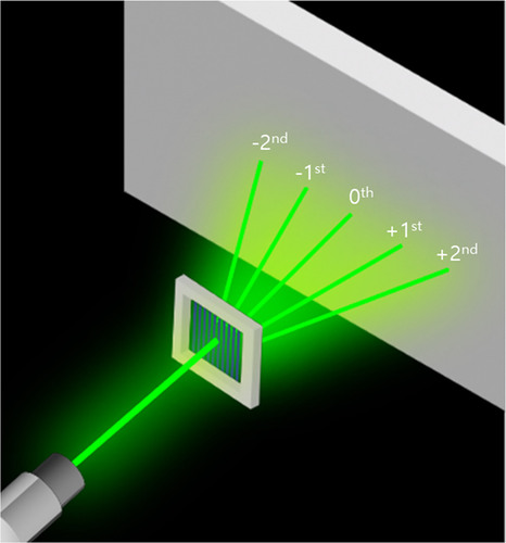
Figure 2. Diffraction angles (dots and line represent simulated and calculated results, respectively) at the first order of the LC grating device as a function of the grating period Λ.
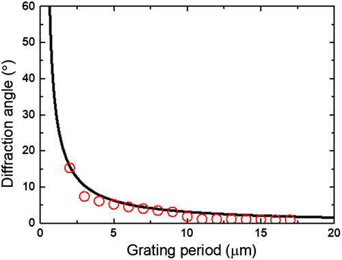
Figure 3. Overview of various LC diffractive grating devices, including LC/polymer composites, photo-aligned LC cells, and LC cells with patterned electrodes.
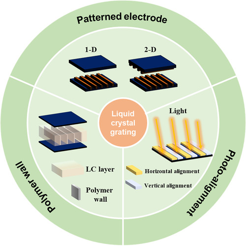
Figure 4. 1-D LC grating device: (a) device structure; (b) calculated LC director distributions; (c) calculated POM images with a full-wave plate; (d) calculated phase difference profiles; and (e) simulated diffraction pattern.
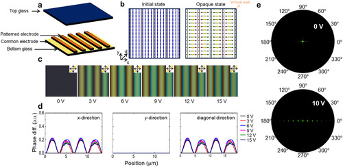
Figure 5. 2-D LC grating device: (a) device structure; (b) calculated LC director distributions; (c) calculated POM images with a full-wave plate; (d) calculated phase difference profiles; and (e) simulated diffraction pattern.
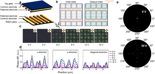
Figure 6. 2-D LC grating device with waffle-shaped electrodes: (a) device structure; (b) calculated LC director distributions; (c) calculated POM images with a full-wave plate; (d) calculated phase difference profiles; and (e) simulated diffraction pattern.
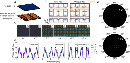
Figure 7. Simulated diffraction pattern of the 1-D, 2-D, and waffle-shaped grating devices.
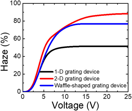
Figure 8. Calculated images of the (a) 1-D, (b) 2-D, and (c) waffle-shaped grating devices with KNU logos.
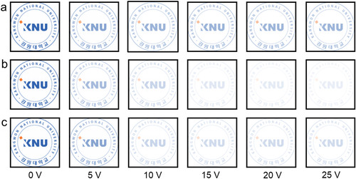
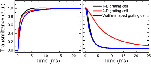
Figure 9. Calculated response time of the 1-D, 2-D, and waffle-shaped grating devices.