Figures & data
Figure 1. XRD patterns of polycrystalline Ge-doped Sb65Se35 (0 ≤ x ≤ 20) alloys.
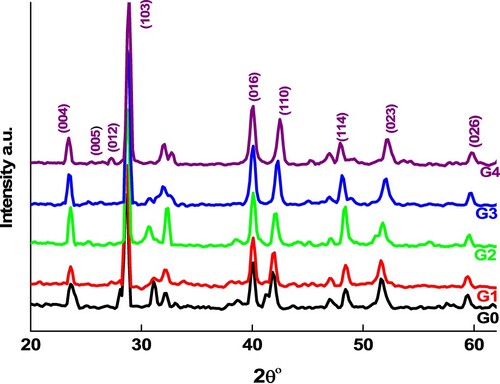
Table 1. EDS, XRD and optical band gap results of the synthesized alloys.
Figure 2. FE-SEM images of the samples were recorded with 20 K x magnification.
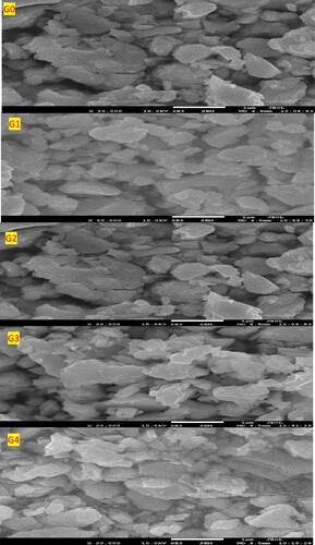
Figure 3. EDS spectra corresponding to the specimens.
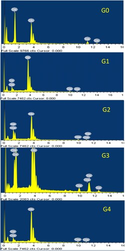
Figure 4. Raman spectra of Ge-incorporated Sb65Se35 (0 ≤ x ≤ 20) samples.
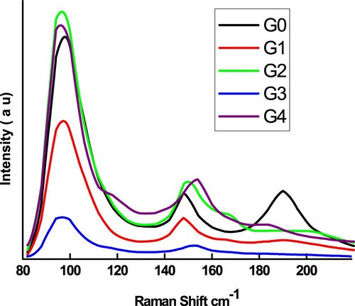
Table 2. The characteristic parameters of each mode, including relative area (A), maximum point position (C), peak widening (W), and relative intensity (I/Io) of Raman peaks of compositions.
Figure 5. Wavelength dependence of the reflectance for all compositions.
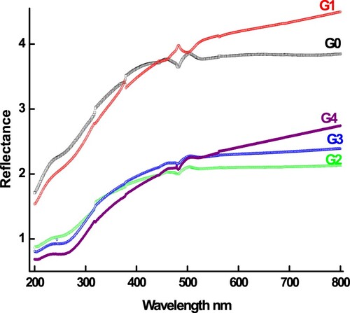
Figure 6. The relationship between the absorption coefficient and energy for various alloys.
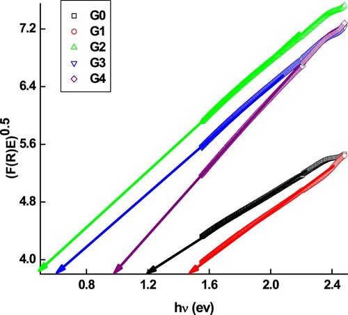
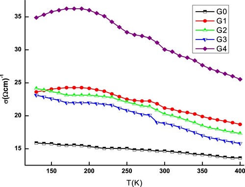
Figure 7. Electrical conductivity (σ) as a function of temperature for various compounds.