Figures & data
Table 1. Arc jet conditions: measured data.
Table 2. Arc jet conditions: derived data.
Table 3. Pyrometer details.
Figure 1. (a) Overview of the as processed SiC/SiC-HfB2 composite. (b) Magnified image of the surface showing the HfB2-SiC and SiC phases in the matrix.
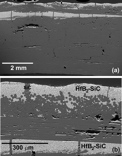
Figure 2. Temperature versus time plot for the four tested samples. The solid lines are the P800 pyrometer and the dotted lines of the corresponding color are the M1000 pyrometer readings. The locations marked SC are where the P800 was switched form dual-colour to single-color mode. The inset images show the surface of the samples after arc jet exposure for each disk.
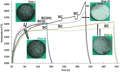
Figure 3. Calculated spectral emissivity at about 1 µm for the considered angle of view (60°) versus temperature measured for Disk I, Disk II and Disk IV. No measurements were taken on Disk III.
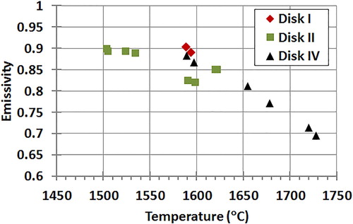
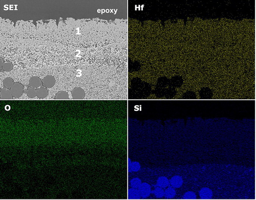
Figure 4. (a) Secondary electron image of the surface of Disk II after arc jet exposure. From the EDS maps for (b) Hf, (c) O and (d) Si, it is shown that there is a thin SiO2-HfO2 layer at the surface which is shown for Disk III in (e). The oxide scale is less than 10 µm and consists of SiO2 (dark phase) and HfO2 (light phase).
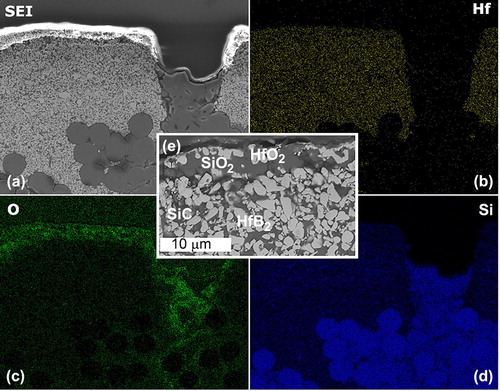
Figure 5. (a) Overview of the oxide scale formed on Disk IV after arc jet exposure. The oxide scale forms three distinct layers 1: porous HfO2; 2: SiC-depleted HfB2 and 3: HfB2-SiC. (b) Surface of the oxide scale. (c) Magnified image of the three layers. SiO2 is not found at the surface in (a), but can be found in some instances as shown in (d).
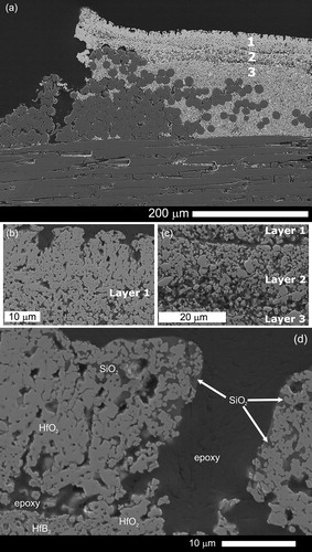
Figure 6. EDS map showing the removal of SiO2 in the outer layer and depletion of SiC from layer 2. Oxygen signal is associated with HfO2.