Figures & data
Figure 1. Non planar substrates schematics (a) Top view of the substrate (b) Cross section schematics of the substrate indicating the gate electrode printing direction (c) Side view schematics illustrating the distinct layers including LIFT printed gate electrodes.
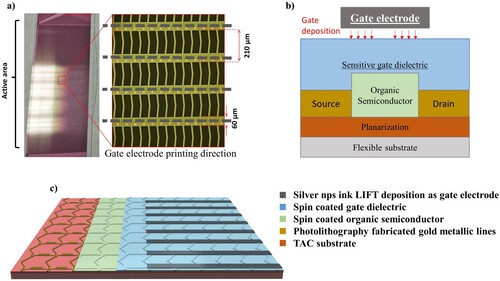
Figure 2. Schematic presentation of laser station (a) Gate electrode laser printing process on top of OTFT stack (b) Gate electrode laser sintering process on top of OTFT stack.
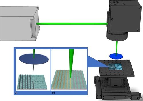
Figure 3. Three nanoparticle inks exhibiting differences regarding the nanoparticle size distribution and the viscosity value and the corresponding scanning electron microscope images (a) ink exhibiting standard nanoparticle size and distribution (Type 1) (b) ink with reduced nanoparticle size and distribution (Type 2) (c) ink with further reduced nanoparticle size and distribution (Type 3).
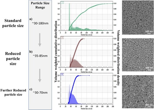
Table 1. Properties of the Ag inks utilised in the experiments.
Figure 4. Resistivity investigation graphs and corresponding scanning electron microscope images of Ag inks films with 1.5 µm thickness (a) Oven temperature baking process and (b) laser sintering process.
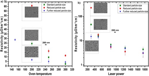
Figure 5. High speed imaging for the evaluation of the rheological behaviour-jetting for (a) standard nanoparticle size ink (b) reduced nanoparticle size ink (c) further reduced nanoparticle size ink.
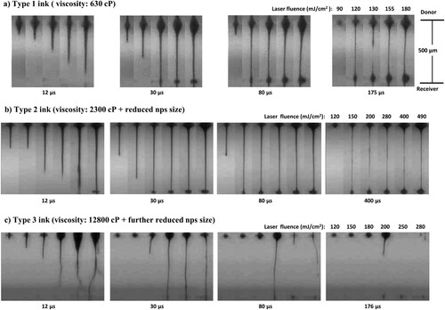
Figure 6. Microscope photos and profile measurements for (a) Type 1 d50 = 70 nm d90 = 120 nm ink (b) Type 2 ink d50 = 56 nm d90 = 71 nm.
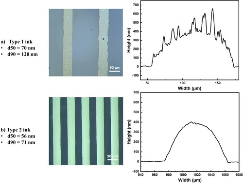
Figure 7. LIFT printed patterns on flexible substrates (a) Demanding design printed on planar flexible dielectric (b) Profile measurements of printed lines.
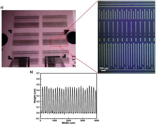
Table 2. Morphological properties and adhesion behaviour of laser printed and laser sintered lines.
Figure 8. LIFT printed patterns on flexible substrates (a) Conformal LIFT printed and sintered 3 cm on non planar flexible substrate (b) Prior to the printing process profile measurement of the non planar substrate (c) corresponding scanning electron microscope image (d) successful connection of the non planar active area with electrical components.
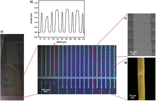
Table 3. Resistivity values comparison for Type 2 ink for laser sintering.
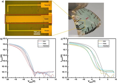
Figure 9. (a) Microscope image of an OTFT device using a laser printed gate (b) Transfer curves measurements for devices with LIFT printed and sintered gate (c) Transfer curves measurements for devices with sputtering deposited gate.