Figures & data
Table 1. Chemical composition of the powder and the as-built parts in wt.%.
Figure 1. Flowchart for the proposed numerical FEM simulation including the experimental route (top) and the simulation route (bottom).
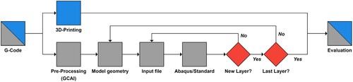
Figure 2. Visualisation of the macroscale (left), combined multiscale (middle) and combined quasi-mesoscale (right) simulation approaches. The macroscale (line equivalent heat source) and mesoscale (Goldak heat source) scan paths are represented by arrows. The powder bed is shown in light grey, the macroscale zone in grey and the mesoscale zone in dark grey.
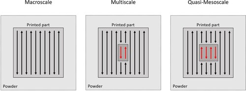
Figure 3. Schematic cut-view representation of the model geometry, split into three regions: combined volume for build plate and powder bed (outside), printed sample and ROI (center).
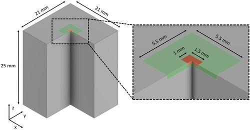
Figure 4. Hierarchical structure used for the material model. Including the material states, solid state phases and tempering states.
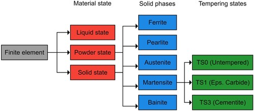
Table 2. The temperature dependence of the variable ‘I’ is characterised by a polynomial function of the form , with the coefficients
and the temperature T, measured in Kelvin (K) taken from Kaiser et al. [Citation36].
Table 3. Thermal input parameters fitted with data from Wilthan et al. [Citation39] and Schwenk et al. [Citation37].
Figure 5. Hardness values of quenched and tempered samples with different heating rates and maximum tempering temperatures plotted over the calculated tempering parameter for each experiment. The linear approximation used for this study is visualised with a dashed line.
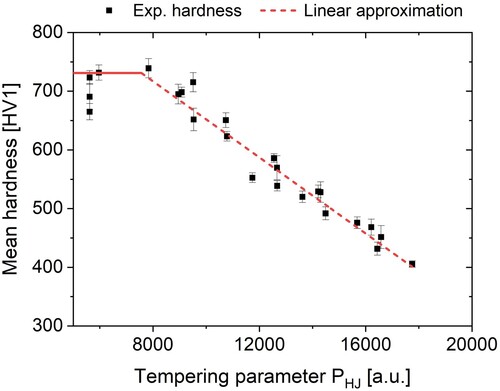
Figure 6. Visualisation of the two optic models used for this study. With the Goldak type optic (a) and the line equivalent optic (b).
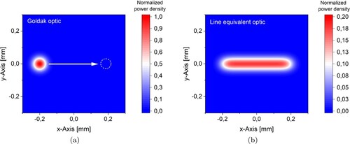
Figure 7. Light microscopic image of a exemplary etched cross section of a single bead printed on top of the sample without additional powder. The effective top surface, the boundary of the hardened zone and the width and depth measurements are highlighted in this image.
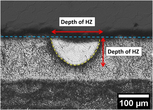
Figure 8. Visualisation of the (a) measured experimental width and depth of HZ of the single beads on top of the printed parts and prediction of width and depth of the HZ of the proposed FEM simulation and (b) direct comparison of experiment and simulation for a LED of .
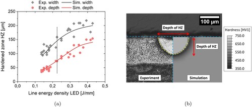
Figure 9. Predicted temperature profile of all three simulation models for a VED of (a) and a VED of
(b).
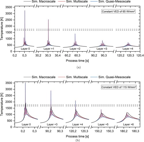
Table 4. Simulation runtime and relative runtime compared to the quasi-mesoscale for all three used simulation approaches.
Figure 10. Predicted mean bulk hardness for different VEDs by the three simulation models compared to experimental data.
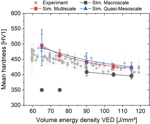
Figure 11. Predicted hardness of a finite element after each layer is printed with a constant VED of 115 Jmm–3. The marked region highlights the crucial time interval for the hardness prediction.
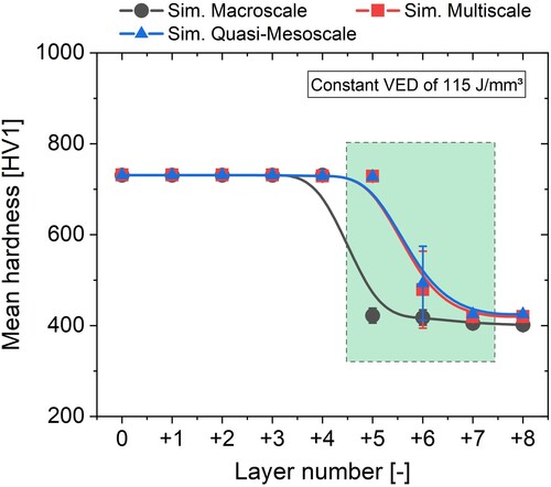
Figure 12. SEM images of the microstructure of the sample with a VED of (a–b) and a VED of
(c–d).
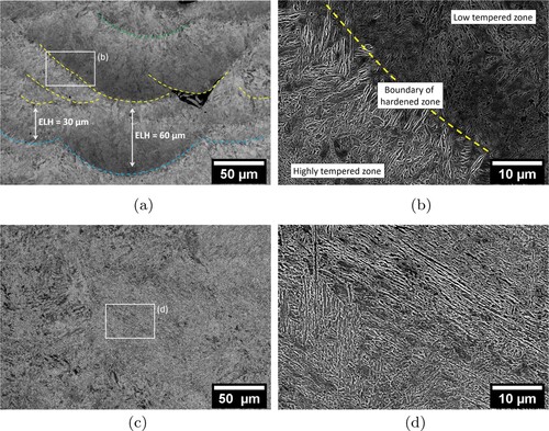
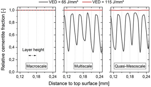
Figure 13. Calculated relative cementite fraction by all three simulation models for the minimum and maximum VED in the printed part. Visualizing local microstructure gradients predicted by the simulation.