
Figures & data
Figure 1. (a) Schematic diagram of the forming process for the DWW technique, where the inset shows that the silver wire is dragged out of the needle tip and is synchronously attached to the stick-on PI film. (b) Basic in-plane wire patterns (square, hexagon and spiral) written along the moving paths. (c) Corresponding moving path and a snapshot of the spatial spanning line structure. (d) Loop circuits containing basic in-plane shapes and spatial spanning structure, inspired by the NFC antenna.
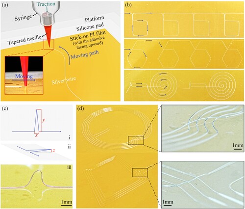
Figure 2. Corner tests in the cases of (a) Dneedle: Dwire = 0.25 mm: 80 μm, and (b) Dneedle: Dwire = 0.25 mm: 20 μm. (c) Definition of manufacturing error. (d) Comparison of the manufacturing errors corresponding to different Dneedle and Dwire in the corner tests (angle: 5° ∼ 150°) under different moving speeds (vspeed: 1 ∼ 9 mm/s).
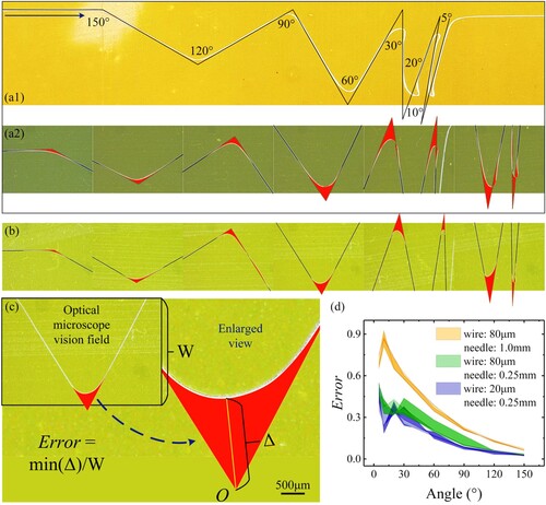
Figure 3. (a) Schematic illustration of the wire-adhesive-substrate sandwich structure along the moving path, where the adhesive interlayer contains weak and strong adhesion regions. (b) Schematic diagram of the top view for the obtuse corners (90° ∼ 180°), where the + x principal moving direction undergoes larger reaction force (namely, the debonding resistance force) compared to the y-axis moving direction. (c) Considerable peeling stress state in the acute corners (<90°) under the -x, y movement components, leading to the debonding of the weak adhesion region near the needle tip more easily.
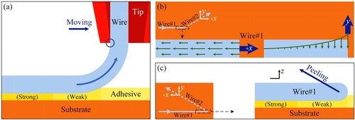
Figure 4. (a) Process steps of 45°-type strain rosette combined with the DWW and DIW techniques. (b) Comparison of testing results between the sensor and DIC method in three strain directions (0°, 45°, 90°) under uniaxial tensile loading. (c) Rapid fabrication of the large-area 5 × 5 sensor array by the same process steps, and (d) the moderate bending compliance of the array.
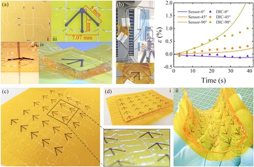
Figure 5. Schematic diagrams of (a) the serpentine (arc radius is 2 mm) wire pattern and (b) the sensor layout in (c) the sensor patch, where the wires marked by red lines will be removed, followed by connecting the intersecting wires and putting the ends of the sensing layers on the electrode pads. (d) The printing process of the serpentine (arc radius is 1 mm) strain sensing layers at the knuckle positions. (e) Electric resistance changes of the sensor patch corresponding to different hand gestures.
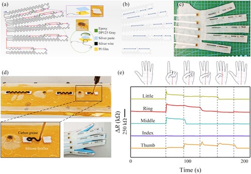
Figure 6. (a) Schematic diagram of the connections between the LED and the middle-severed serpentine (arc radius is 2.5 mm) wire via silver paste. Simple flexible LED device under (b) bending and (c) stretching (strain: 0 ∼ 36%). Complex light display array containing (d) the row/column wire pattern and (e) the red/blue LEDs arranged along characters ‘JN’, exhibiting the tolerant capability for bulging and bending. (f) Controllable luminescence of LED units inside character ‘N’ by turning on/off the corresponding circuit separately.
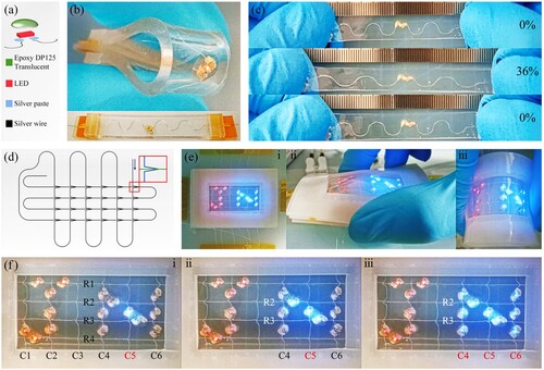
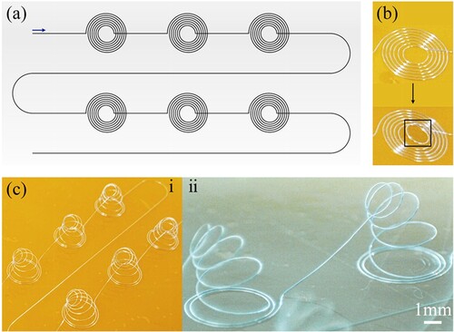
Figure 7. (a) Schematic illustration of the in-plane linear spirals (radii: 1.2 ∼ 3 mm, spacing: 0.3 mm) on PI film. (b) Warping at the central smallest curve. (c) Spatial helixes formed by the accelerated warping under 85 °C, showing the repeatable and stable shape.
Supplemental Material
Download PDF (4.3 MB)Data availability statement
The authors confirm that the data supporting the findings of this study are available within the article and its supplementary materials.