
Figures & data
Table 1. Main experimental conditions.
Figure 1. Printing process of CCLE: (a) schematic of CCLE; (b) voxel-by-voxel printing.
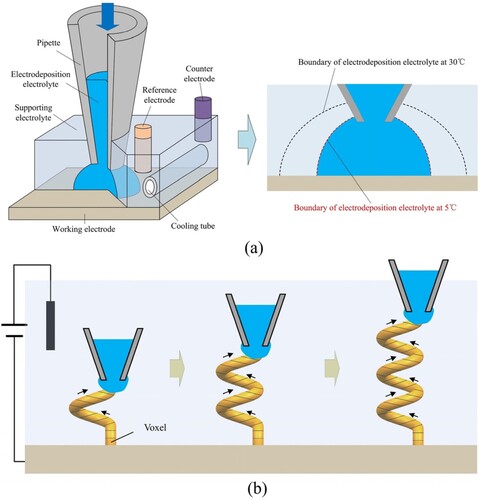
Figure 2. Microscale diffusion process of the electrodeposition electrolyte in the supporting electrolyte: (a) printing setup; (b) printing cell; (c) nanopipette; (d) diffusion at different temperatures.
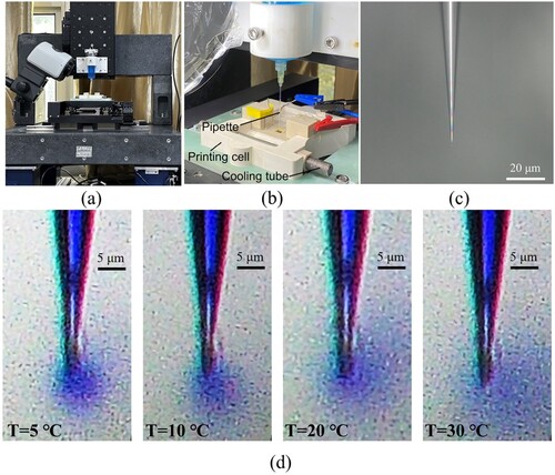
Figure 3. Voltammetry of the electrodeposition electrolyte at different temperatures, as well as the supporting electrolyte.
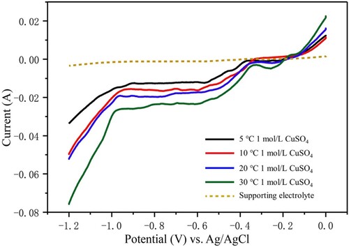
Figure 4. SEM images of the printed deposits obtained in the electrolytes at temperatures of (a) 30 °C, (b) 20 °C, (c) 10 °C, and (d) 5 °C.
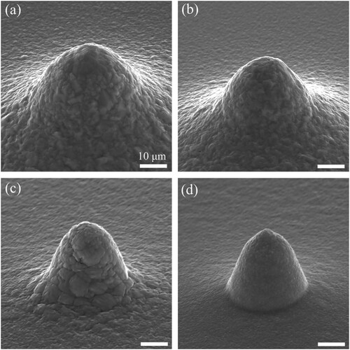
Figure 5. Transmission electron microscopy (TEM) images of the printed deposits obtained in the electrolytes at temperatures of 30, 20, 10, and 5 °C.
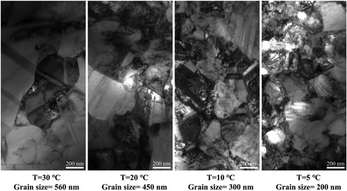
Figure 6. Effects of the potential and pressure on printing via the CCLE technique: (a) SEM images of the printed pillars; (b) ratio of the top diameter to the bottom diameter (dt/db) for the pillars obtained with different parameters; (c) magnified SEM micrographs of pillars printed at –0.7 V and 1, 3, and 5 mbar.
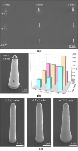
Figure 7. (a) Print rate and (b) volumetric rate of the CCLE technique.
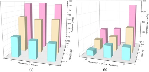
Figure 8. EDX spectrum of the printing deposits
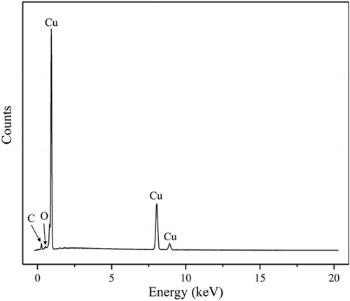
Figure 9. FIB-SEM (a) longitudinal section and (b) transverse section images of the printed pillars at −0.7 V and 1 mbar.
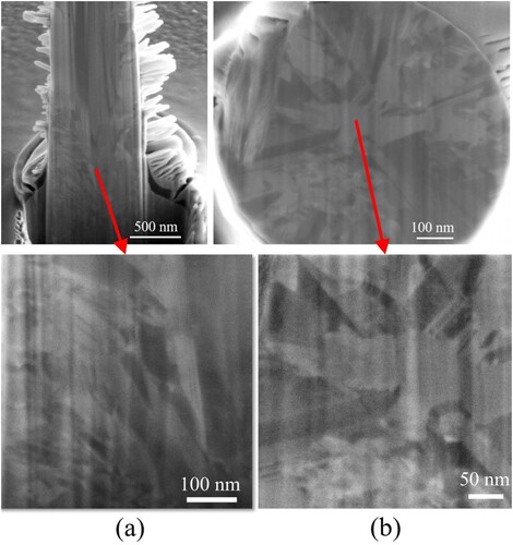
Figure 10. SEM images of the printed (a) helix at 30 °C with pressure of 1 mbar, (b) helix at 5 °C with pressure of 1mbar, (c) pillars with a high aspect ratio at 5 °C, (d) helix at 30 °C with pressure of 10 mbar and (e)helix at 5 °C with pressure of 10 mbar.
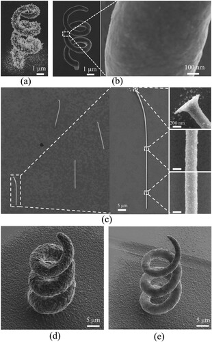
Figure 11. In-situ SEM micro-compression experiment on Cu pillars printed at different temperatures: (a) pillar printed at 30 °C, (b) pillar printed at 5 °C, (c) the stress and the depth of the diamond tip in the experiment.
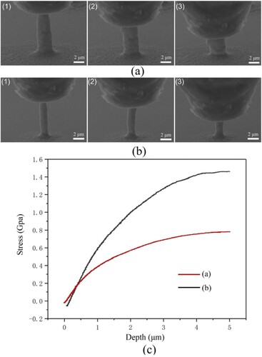
Table 2. Published descriptions on MCED and FluidFM and corresponding descriptions on CCLE.
Data availability statement
Data available on request from the authors.