
Figures & data
Figure 1. .#Workflow of the proposed method.
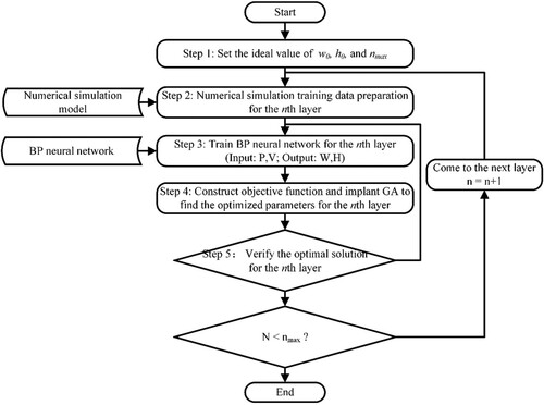
Figure 2. (a, b) The FE model of the multi-layer LPBF process and (c) laser scanning pattern during.
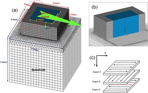
Figure 3. BP neural network model.
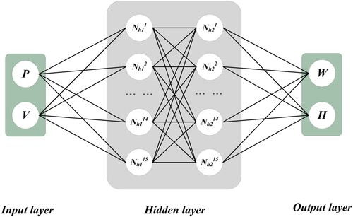
Table 1. Finite element simulation process parameters.
Table 2. Material parameters of solid Invar.
Table 3. Thermal property parameters of solid Invar.
Figure 4. (a) Invar alloy LPBF single pass scanning forming sample diagram. (b) The 16th group of samples melt track morphology.
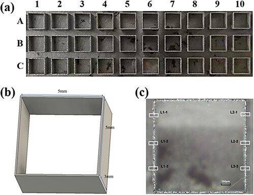
Table 4. Laser processing parameters for single tracks simulation and printing.
Figure 5. Numerical simulation and experimental values of the width of the melt track of stabilized working layer during LPBF of Invar alloy power process using different laser power (V = 800 mm/s) (a) and scanning speed (P = 140 W) (b).
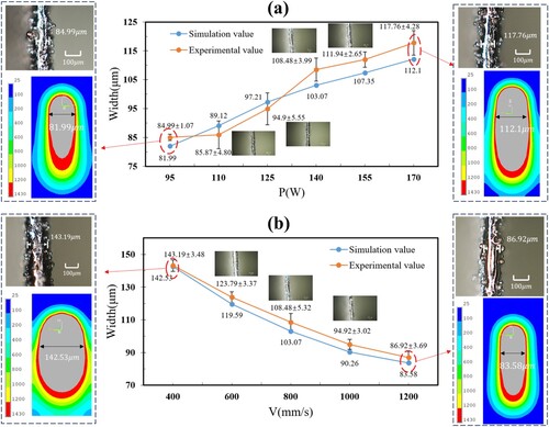
Figure 6. The loss curve of neural network.
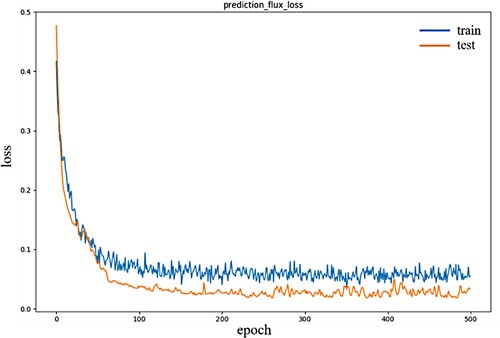
Figure 7. Sample value and BP neural network output value.
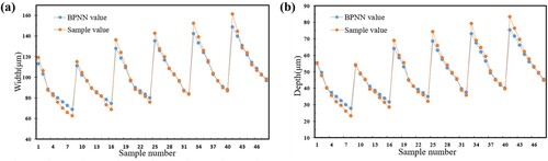
Figure 8. Test value and BP neural network output value.
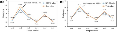
Table 5. Layer-by-layer optimization results.
Figure 9. Comparison between layer-by-layer optimized process parameters and mono process parameters.
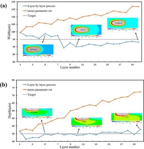
Figure 10. The boxes with different heights used in the printing experiment.
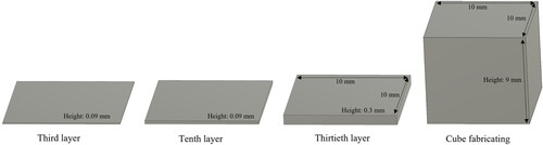
Table 6. LPBF cubic fabricating process parameters.
Figure 11. The relationship between surface roughness and input energy density and the number of processing layers.
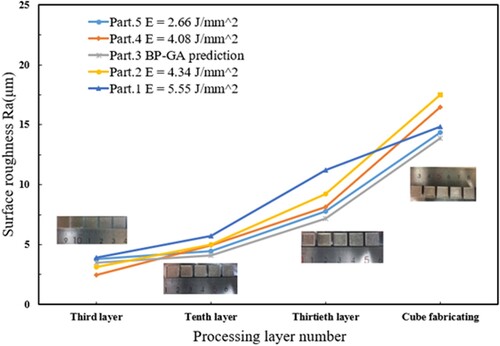
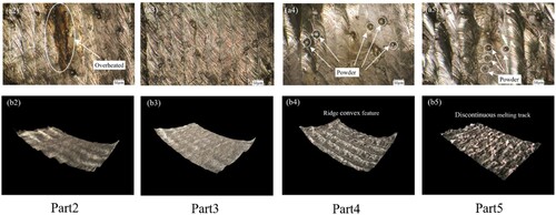
Figure 12. The typical topography and three-dimensional scan image of the upper surface of the cube sample made with the process parameters in observed with an ultra-depth-of-field microscope.
Data availability statement
The data that support the findings of this study are available from the corresponding author [Y. Zhang], upon reasonable request.