
Figures & data
Figure 1. Schematic diagrams of fabrication of electrochemically coated WS2 modified 3D-printed carbon electrode for fabrication of symmetric supercapacitors.
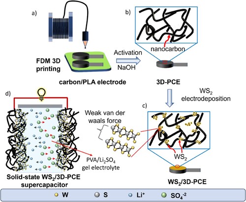
Figure 2. Scanning electron microscopy (SEM) image of (a, b) blank 3D-PCE (inset: digital image of the electrode after activation; scale 5 mm), (c, d) WS2/3D-PCE, (e) SEM-energy dispersive X-ray (EDX) spectroscopy mapping area and (f–j) elemental mapping of W, S, O, C and overlay respectively of WS2/3D-PCE, respectively.
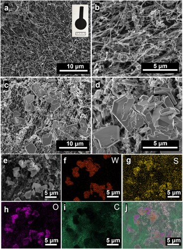
Figure 3. X-ray photoelectron spectroscopy (XPS). High-resolution core-level spectra of (a) W 4f and (b) S 2p of WS2/3D-PCE.
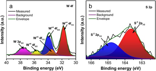
Figure 4. Electrochemical study in the three-electrode system (a) comparison of WS2/3D-PCE and 3D-PCE at 50 mV s−1, (b) specific capacitance comparison, (c) cyclic voltammogram of WS2/3D-PCE at different scan rates, (d) galvanostatic charge-discharge curves of WS2/3D-PCE at different current densities 0.178, 0.255 and 0.764 mA cm−2 which is labelled as I, II, and III, respectively.
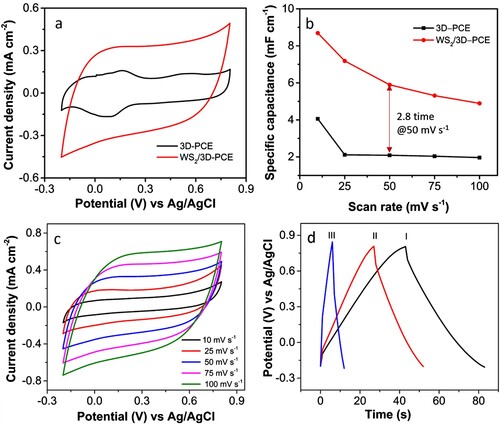
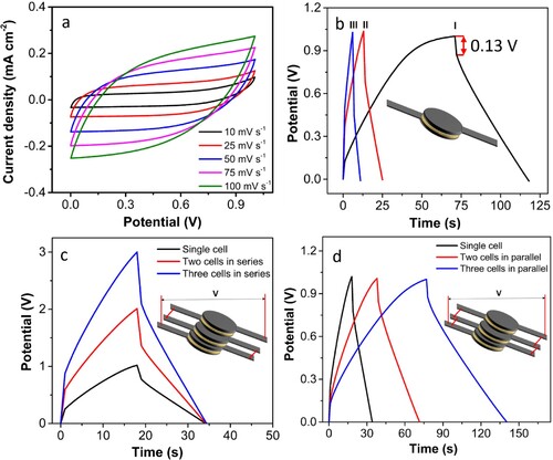
Figure 5. Electrochemical study in two electrode system. (a) Cyclic voltammogram of WS2/3D-PCE solid-state symmetric supercapacitor at different scan rates (b) galvanostatic charge-discharge (GCD) curves of WS2/3D-PCE solid-state symmetric supercapacitor at different current densities 56.62, 169.87, and 283.09 µA cm−2, denoted as I, II, and III, respectively. GCD curves of (c) series and (d) parallel connection of two and three-cells at the current density of 0.11 mA cm−2, respectively.
Supplemental Material
Download MS Word (3.1 MB)Data availability statement
The data that support the findings of this study are available from the corresponding author, M. P., upon reasonable request.