
Figures & data
Figure 1. Schematic of experimental setup for WAAM system with integration of GTAW and CMT processes.
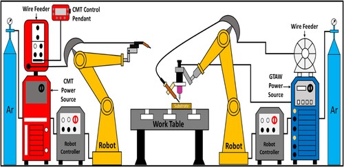
Table 1. Chemical composition (wt.-%) of In625 consumable wire and 90WNiFe substrate.
Figure 2. (a)–(c) Thin walls of 90WNiFe/In625 BS fabricated with various heat inputs, (d) deposition strategy, and (e) tensile specimen dimensions.
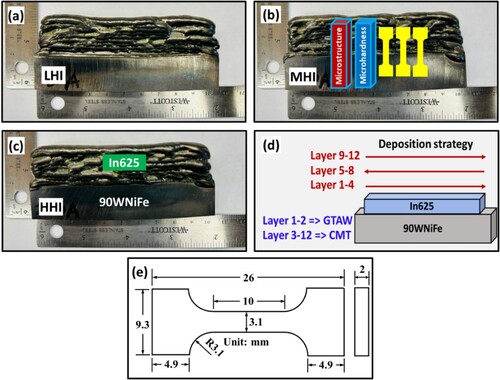
Table 2. Layer-wise process parameters for different heat input conditions.
Figure 3. Optical microscopy images of 90WNiFe/In625 BS for LHI, MHI, and HHI conditions: Micrograph of the thin walls (a, e, i); In625 side (b, f, j); Interface (c, g, k); and 90WNiFe side (d, h, l).
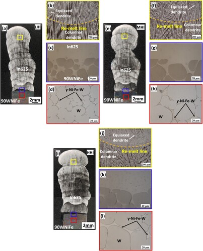
Figure 4. For the LHI, the SEM images depicting: (a) In625 side adjacent to the interface, (b) 90WNiFe/In625 interface and corresponding EDS elemental area mapping, and (c) 90WNiFe side adjacent to the interface; (d) EDS line scan performed at the interface indicated in Figure (b) by the black dashed line, and (e) EDS point scan results at the locations shown in Figure (a, b, c).
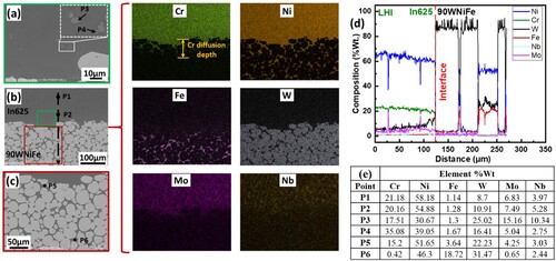
Figure 5. For the MHI, the SEM images depicting: (a) In625 side adjacent to the interface, (b) 90WNiFe/In625 interface and corresponding EDS elemental area mapping, and (c) 90WNiFe side adjacent to the interface; (d) EDS line scan performed at the interface indicated in Figure (b) by the black dashed line, and (e) EDS point scan results at the locations shown in Figure (a, b, c).
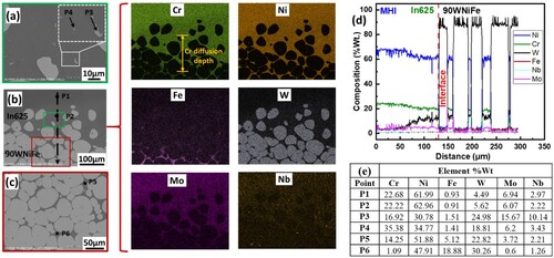
Figure 6. For the HHI, the SEM images depicting: (a) In625 side adjacent to the interface, (b) 90WNiFe/In625 interface and corresponding EDS elemental area mapping, and (c) 90WNiFe side adjacent to the interface; (d) EDS line scan performed at the interface indicated in Figure (b) by the black dashed line, and (e) EDS point scan results at the locations shown in Figure (a, b, c).
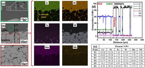
Figure 7. (a) Magnified SEM image for inset of (a) along with EDS scan location indicated by line AB and (b) line scan data showing compositional variation along line AB.
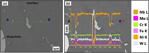
Figure 8. (a) Equilibrium-cooling phase calculation of 50:50 mixture (by weight) of 90WNiFe and In625; XRD Results for (b) Interface (LHI, MHI, and HHI conditions), (c) 90WNiFe side, and (d) In625 side.
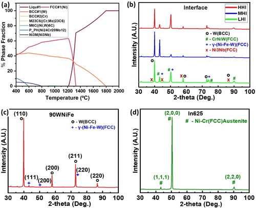
Figure 9. Microhardness profiles for (a) LHI thin-wall, (b) MHI thin-wall, (c) HHI thin-wall, and (d) comparison of the microhardness at various locations of 90WNiFe/In625 thin-wall.
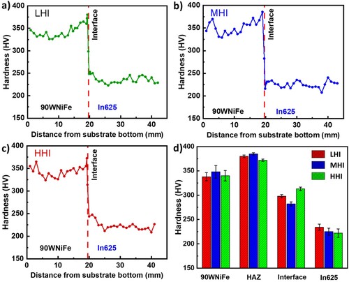
Figure 10. Stress-strain curve: (a) LHI, (b) MHI, and (c) HHI; (d) Comparison of Avg. YS, UTS, and elongation.
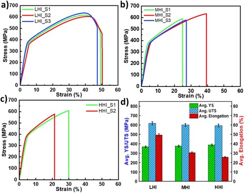
Table 3. Summary of the tensile test results for different conditions.
Figure 11. (a)–(c) Fractured samples; SEM images of fractured tensile samples: LHI (a1–a3), MHI (b1–b3), and HHI (c1–c3).
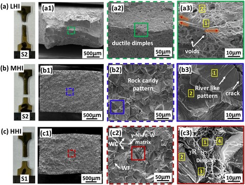
Table 4. EDS point scan results of fracture surfaces of tensile samples for different heat input conditions.
Figure 12. Bonding mechanism of 90WNiFe/In625 during wire-arc DED process.
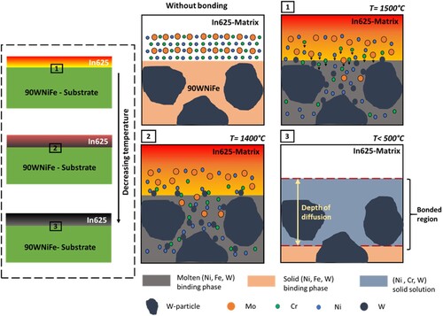
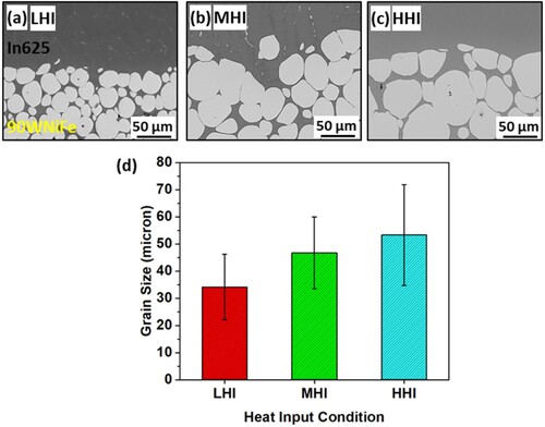
Figure 13. SEM Images of BS interface: (a) LHI, (b) MHI, (c) HHI, and (d) comparison of W grain size.
Data availability statement
Authors agree to make data and materials supporting the results or analyses presented in their paper available upon reasonable request.