
Figures & data
Figure 1. (a) The SEM map, (b) particle size distribution and (c) associated EDS mapping results of the mixed AlMo0.25FeCoCrNi2.1 powders. The inserted image in (a) is the high-magnification SEM map of pure Mo particles.
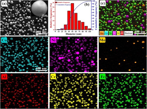
Figure 2. (a) Schematic diagram of the multilayer LDED process with a zigzag scanning strategy, (b) the geometrical descriptions of the LDEDed thin-wall build and tensile samples.
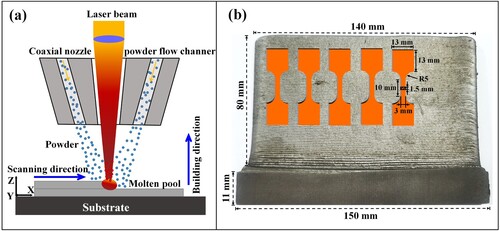
Figure 3. (a) XRD patterns of AlMo0.25FeCoCrNi2.1 HEA with various annealing times, (b) the local amplified of the 2θ ranging from 38° to 50°.
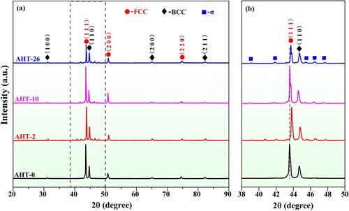
Figure 4. (a) Three-dimensional and (b) X-Z section OM observations of the microstructure in as-deposited AlMo0.25FeCoCrNi2.1 alloy. (c) High-magnification SEM image and (d) associated EDS results of the microstructure selected in the middle region of banded layers shown in (b).
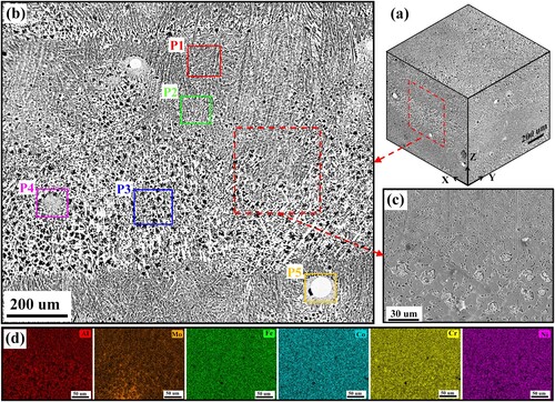
Figure 5. (a) The IPF map, (b) GND density map and (c) average grain size of the as-deposited AlMo0.25FeCoCrNi2.1 microstructure. (d) The high-magnification IPF map, (e) phase map and (f) IPFs of amplified region from (a).
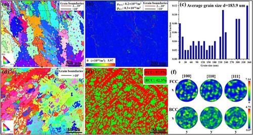
Figure 6. SEM maps and associated EDS mapping results of representative regions (a) P1, (b) P2, (c) P3, (d) P4 and (e) P5 in as-deposited microstructure shown in .
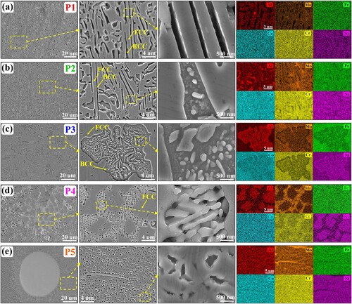
Figure 7. (a) TEM map, (b) associated EDS mapping results and (c) SAED patterns of flower-like structure of microstructure in region P3 shown in (c).
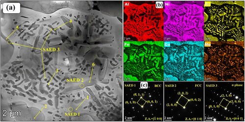
Table 1. EDS point results of structures in region P3 (at. %).
Figure 8. (a) TEM maps, (b) EDS mapping results and (c) SAED patterns of nanoscale lamellar structure in region P4 shown in (d).
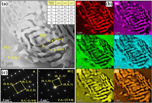
Figure 9. Schematic illustration of the dynamic melting-solidification process of during the LDED of AlMo0.25FeCoCrNi2.1 HEA.
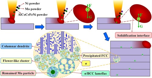
Table 2. Atomic size, melting points, density and mixing enthalpy of elements in mixed AlMo0.25FeCoCrNi2.1 HEA.
Figure 10. The SEM maps and associated EDS results of annealed microstructure in the representative regions (a)-(c) P2, (d)-(f) P3 and (g)-(i) P4.
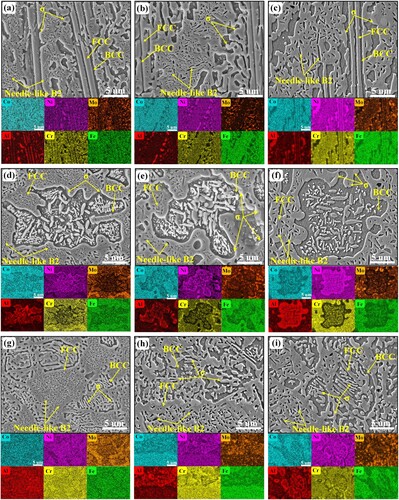
Figure 11. (a) TEM map, (b) high-magnification TEM map, (c) associated EDS test results and (d) associated SAED patterns and HRTEM images of coarse FCC phases in region P2 of AHT-26 sample.
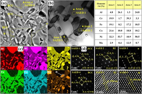
Figure 12. (a) TEM map, (b) high-magnification TEM map, (c) associted EDS test results and (d) associated SAED patterns and HRTEM images of fine FCC/BCC eutectic structures in region P2 of AHT-26 sample.
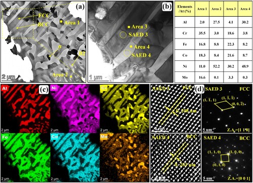
Figure 13. (a) TEM map, (b) local amplified TEM map, (c) EDS mapping results and (d) SAED patterns of flower-like structures and precipitations in region P3 of AHT-26 sample.
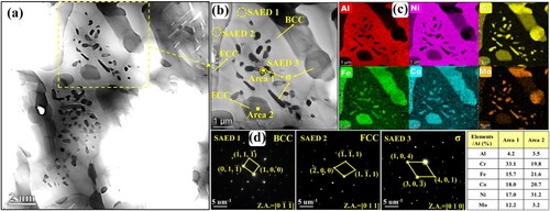
Figure 14. The hardness variations of as-deposited and annealed AlMo0.25FeCoCrNi2.1 samples.
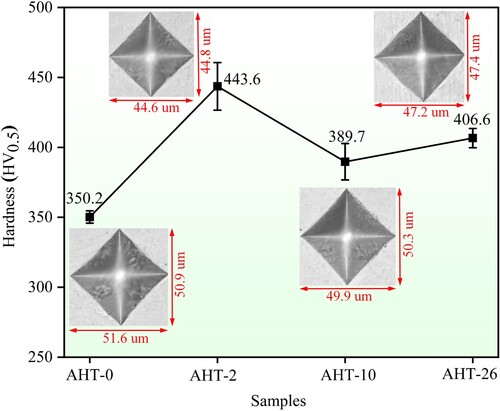
Figure 15. The tensile stress-strain curves of as-deposited and annealed AlMo0.25FeCoCrNi2.1 samples.
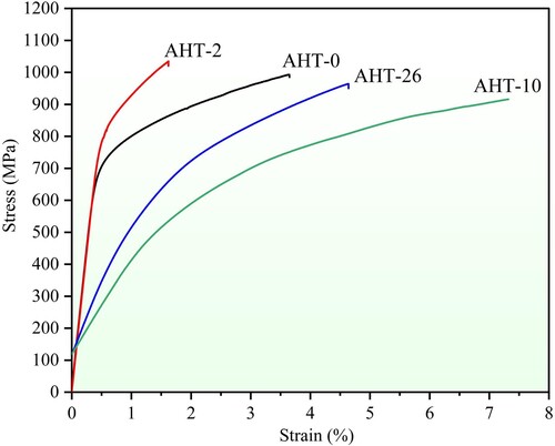
Table 3. Tensile properties of AlMo0.25FeCoCrNi2.1 HEA at room temperature.
Figure 16. The tensile fracture morphologies of (a)-(b) AHT-0, (c)-(d) AHT-2, (e)-(f) AHT-10 and (g)-(h) AHT-26 samples. (i) and (j) are the high-magnification SEM map and associated EDS mapping results of bare Mo particles in (a). (k) and (l) are the high-magnification SEM maps of selected regions in (g) and (h), respectively.
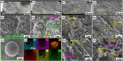
Figure 17. (a) Kinetic potential polarisation curves, (b) Bode plots, (c) Nyquist plots and (d) Equivalent circuit of as-deposited and annealed AlMo0.25FeCoCrNi2.1 samples.
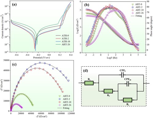
Table 4. Electrochemical corrosion parameters of as-deposited and annealed AlMo0.25FeCoCrNi2.1 samples.
Table 5. Equivalent circuit parameters of impedance spectra of as-deposited and annealed AlMo0.25FeCoCrNi2.1 samples.
Figure 18. Corrosion surface morphologies and associated EDS mapping results of high-magnification regions of (a) AHT-0, (b) AHT-2, (c) AHT-10 and (d) AHT-26 samples after kinetic potential polarisation test.
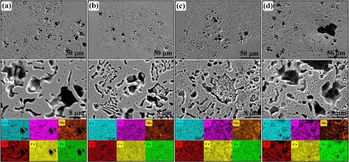
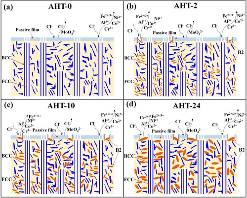
Figure 19. Schematic illustration of the destroy mechanism of passive film completeness on the FCC phase by precipitated needle-like B2 phases during the annealing heat treatment.
Data availability statement
The authors declare that all data supporting the findings of this study are available within the paper.