Figures & data
Figure 1. (Colour online) Schematic diagram of ion etched tracks inside the Si substrate filled by: (a) Co–Pt alloys and (b) multilayer nanowires.
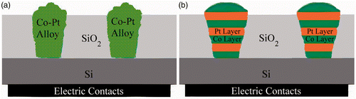
Figure 2. Current-time profile for growing of Co/Pt multilayer.
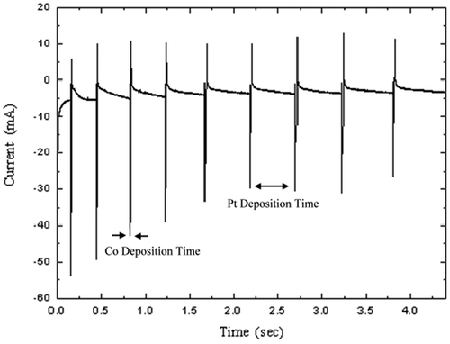
Figure 3. (a) SEM image of a substrate surface after filling the pores with Co–Pt nanowires. (b) EDAX spectrum of the sample.
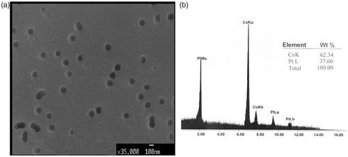
Figure 4. Hysteresis loop of: (a) Co–Pt alloy and (b) [Co(5 nm)/Pt(3 nm)] multilayer. Magnetic field is applied parallel to the sample surface.
![Figure 4. Hysteresis loop of: (a) Co–Pt alloy and (b) [Co(5 nm)/Pt(3 nm)] multilayer. Magnetic field is applied parallel to the sample surface.](/cms/asset/95881b7e-8b51-4b69-87c5-2de12a8f4e8f/tjen_a_654273_o_f0004g.gif)
Figure 5. The schematic of experimental set up for MR measurements.
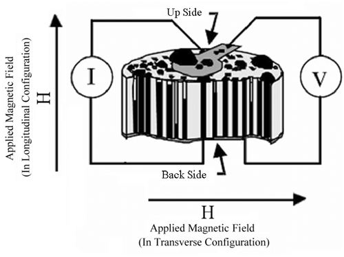
Figure 6. Transverse (a) and longitudinal (b) magnetoresistance for a [Co(5 nm)/Pt(3 nm)] multilayer nanowire.
![Figure 6. Transverse (a) and longitudinal (b) magnetoresistance for a [Co(5 nm)/Pt(3 nm)] multilayer nanowire.](/cms/asset/0bb83caa-fec8-4c87-87fe-c343854c14cd/tjen_a_654273_o_f0006g.gif)
Figure 7. Transverse (a) and longitudinal (b) magnetoresistance for a Co–Pt alloy nanowire.
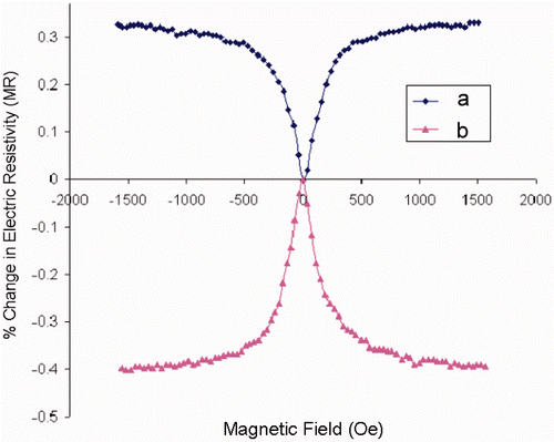
Figure 8. EDAX spectrum for a Co–Pt alloy nanowire.
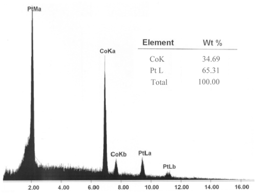
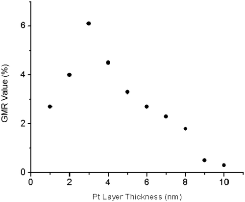
Figure 9. GMR as a function of Pt layer thickness for a series of nanowires with similar Co thickness of 5 nm.