Figures & data
Figure 1. XRD patterns of Bi1.05Fe1− x Mn x O3 (x = 0, 0.01, 0.02, 0.03, 0.04 and 0.05) thin films deposited on ITO/glass substrates.
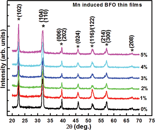
Figure 2. Magnified XRD patterns of BiFe1− x Mn x O3 (x = 0, 0.01, 0.02, 0.03, 0.04 and 0.05) thin films in the vicinity of 2θ = 32° showing merging and shifting of (104) and (110) diffraction peaks towards higher angle.
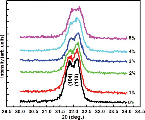
Figure 3. Room-temperature unpolarised Raman spectra of BiFe1− x Mn x O3 (x = 0, 0.01, 0.02, 0.03, 0.04 and 0.05) thin films deposited on silicon (100) substrates.
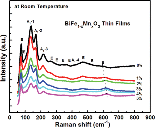
Figure 4. Room-temperature (M–H) hysteresis loop of BiFe1− x Mn x O3 (x = 0, 0.01, 0.02, 0.03, 0.04 and 0.05) thin films deposited on silicon (100) substrates, in which inset shows the variation in M s with Mn-doping concentration.
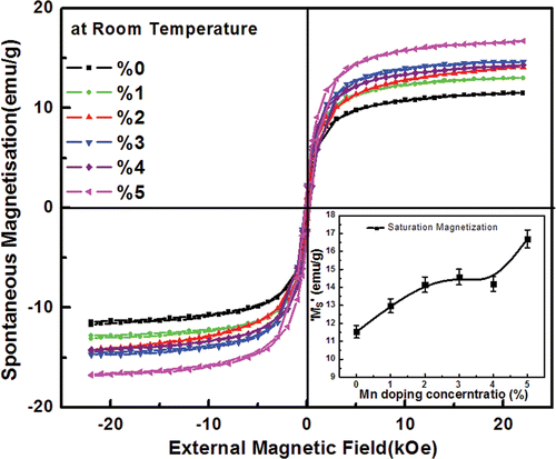
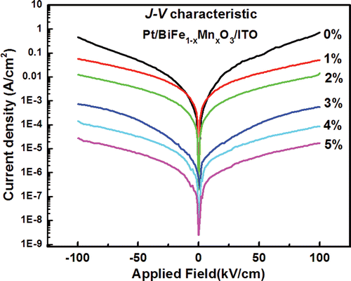
Figure 5. Leakage current density–electric field (J–E) curves (semilogarithmic plot) of Pt/BiFe1− x Mn x O3/ITO/glass (x = 0, 0.01, 0.02, 0.03, 0.04 and 0.05) thin-film capacitors.