
Figures & data
Figure 1. TEM images of AuNSs. (a) 15 nm and (b) 30 nm.
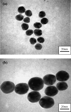
Figure 2. Histograms of distribution of particles size. (a) 15 nm AuNSs and (b) 30 nm AuNSs.
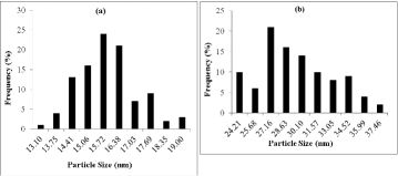
Table 1. Average length, average diameter and aspect ratio of AuNRs measured from TEM images.
Figure 3. TEM micrographs of AuNRs. (a) 3.12 aspect ratio, (b) 3.39 aspect ratio and (c) 3.60 aspect ratio.
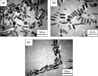
Table 2. Surface coverage density of various AuNSs coatings thin films.
Figure 4. SEM images. (a) 1 coating, (b) 3 coatings and (c) 5 coatings of 15 nm AuNSs, (d) 1 coating, (e) 3 coatings and (f) 5 coatings 30 nm AuNSs thin film on Si substrates.
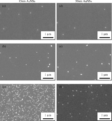
Figure 5. Schematic diagram of structure Si/AuNPs/Ag.
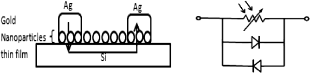
Figure 6. Schematic diagram of structure Si/Ag.
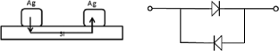
Figure 7. The current–voltage (I–V) curves of the control sample in light–dark conditions.
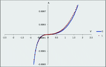
Figure 8. The current–voltage (I–V) curves in light (L) and dark (D) conditions of various coatings of thin films on Si substrate: (a) 15 nm AuNSs solution and (b) 30 nm AuNSs solution.
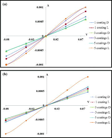
Table 3. Surface coverage density of various AuNRs coatings thin film.
Figure 9. SEM micrographs with various coatings of different aspect ratio AuNRs thin film on Si substrate. (a)–(c) 1, 3, 5 coatings of 3.12 aspect ratio AuNRs, (d)–(f) 1, 3, 5 coatings of 3.39 aspect ratio AuNRs and (g)–(i) 1, 3, 5 coatings of 3.60 aspect ratio AuNRs.
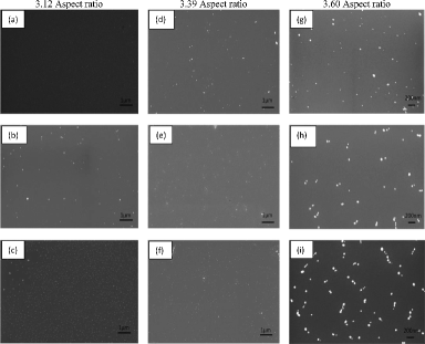
Figure 10. The current–voltage (I–V) curves in light (L) and dark (D) conditions of various coatings of different aspect ratios AuNRs thin films on Si substrates: (a) 3.12, (b) 3.39 and (c) 3.60 aspect ratios AuNRs.
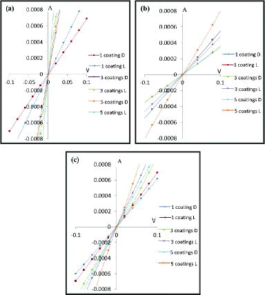
Table 4. Resistance and sensitivity with varying coating layers of different size AuNSs and AuNRs thin film.