Figures & data
Figure 1. (a) General morphology of deposits, (b) magnified SEM image of the crowded nanoplates.
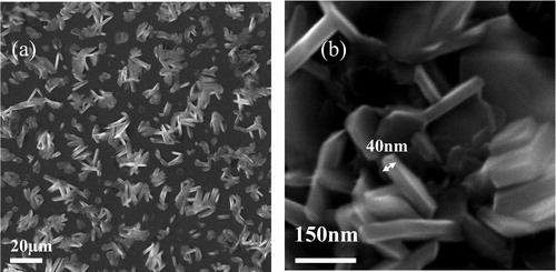
Figure 2. (a) Morphology of nanoplates grown at 760 °C for 1 min, (b) TEM image of a single nanoplate, (c) high resolution TEM image, (d) SAED pattern, (e) EDAX spectrum of a nanoplate, (f) AFM image of nanoplates, (right) height plot crossing an edge of a small nanoplate.
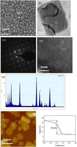
Figure 3. SEM image of nanoplates grown on a TEM grid.
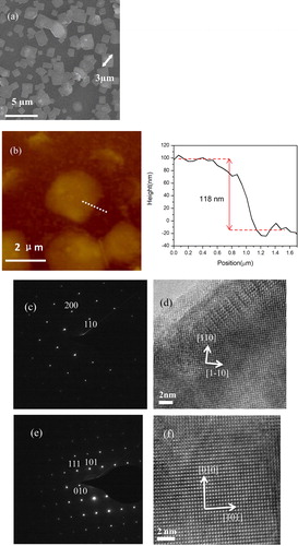
Figure 4. (a) Morphology of nanoplates grown with decaborane addition, (b) AFM image of nanoplates, (right) height plot crossing an edge of a nanoplate, (c) and (e) SAED pattern, (d) and (f) high resolution TEM image of the same nanoplate in different zone axis.
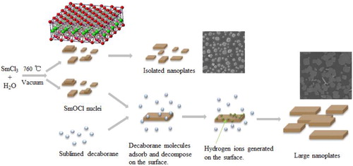
Scheme 1. Schematic illustration of SmOCl nanoplate formation. SmOCl Structure: Bi (pink), O (red), Cl (green).