Figures & data
Figure 1. Structure of the fluorine-based block-co-polymer used as a precursor for the preparation of TFD-co-TFE films by wet chemical spin coating process
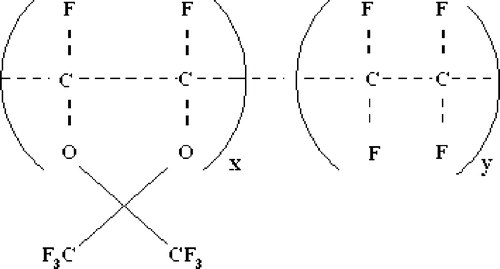
Figure 2. Flow chart for the preparation and deposition of TFD-co-TFE thin films by wet chemical spin coating process
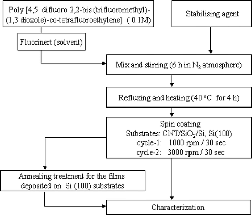
Figure 3. SEM image and EDX spectrum of TFD-co-TFE film deposited on Si(100) at room temperature by sol--gel spin coating process
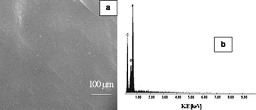
Figure 4. SEM image and EDX spectrum of TFD-co-TFE film deposited on Si(100) by sol--gel spin coating process and annealed at 400°C for 1 h
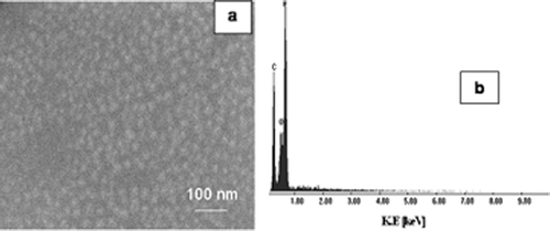
Figure 5. SEM image of vertically aligned CNT on Ni nanoparticles on SiO2/Si substrate grown at 750°C by radio frequency pulsed plasma chemical vapor deposition technique
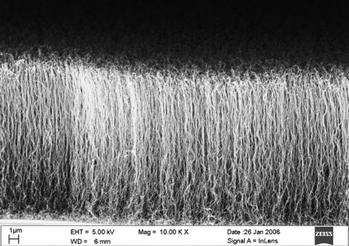
Figure 6. AFM topographical images of TFD-co-TFE thin films on Si(100) substrate by sol--gel spin coating process (a) As deposited (xerogel) film and (b) xerogel film annealed at 400°C/1 h (scan area 1 µm × l µm, Z axis = 100 nm)
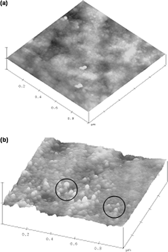
Figure 7. SEM planar view of the vertically aligned CNT coated with hydrophobic ultra thin film (5 nm) (TFD-co-TFE)
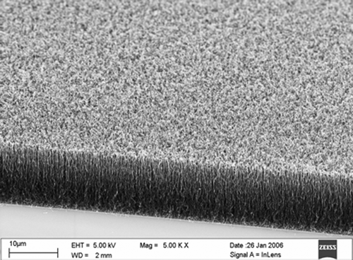
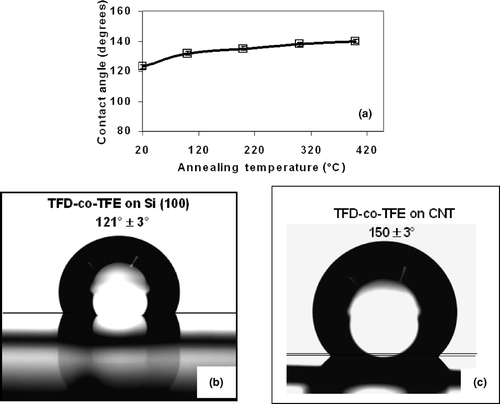
Figure 8. (a) Water contact angles vs. annealing temperatures of TFD-co-TFE films deposited on Si(100). Water droplet picture taken during measurement at room temperature (b) TFD-co-TFE film coated on Si(100) and (c) TFD-co TFE film coated on CNT/SiO2/Si