Figures & data
Figure 1. Cross section of D-MEMS in passive state (upper left) and actuated state (lower left), with their corresponding diffraction patterns (right).
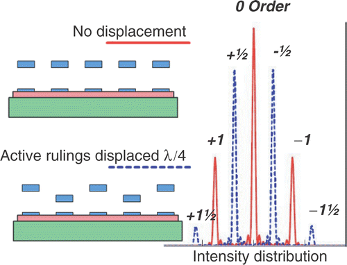
Figure 2. Schematic of ruling.
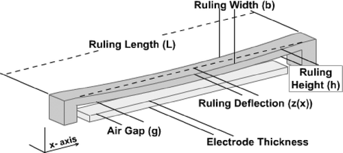
Table 1. Dimensions of rulings used in capacitance simulations.
Table 2. Constants for electrostatic force including fringe-field effect.
Figure 3. Comparison of analytical equations and simulation of electrostatic force as function of air gap for 2 µm wide ruling-electrode model.
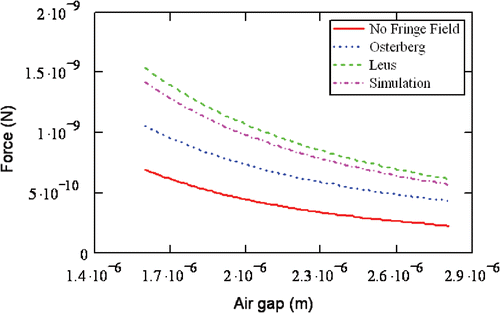
Figure 4. Schematic (not to scale) of: (a) Double-Clamped design, (b) Cantilever-Suspension design, and (c) Double Grating design.
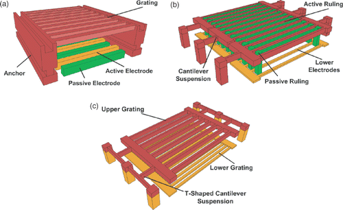
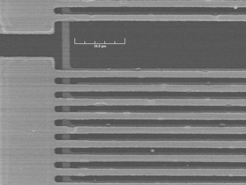
Figure 5. Double-Clamped device results: (a) SEM image showing the anchor and rulings, (b) WLI result showing 80 nm centre ruling buckling on average.
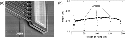
Figure 6. Switching behaviour of Double-Clamped device.
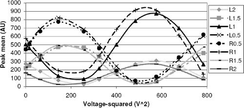
Figure 7. WLI result of cantilever-suspension design showing difference in buckling due to residual stress of passive (upper) and active (lower) rulings.
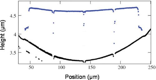
Figure 8. Optical switching results of Cantilever-suspension design.
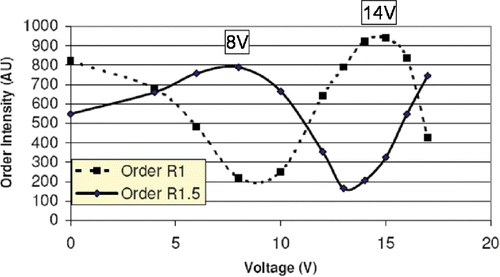
Figure 9. Laser vibrometer results of double-grating design, at 12V applied potential.

Figure 10. Optical test results of double grating design.
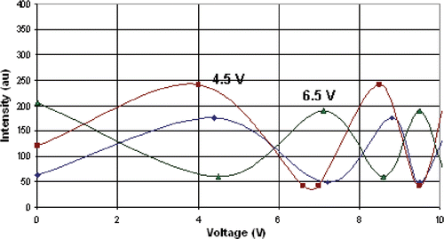
Figure 11. Polyimide D-MEMS process flow.
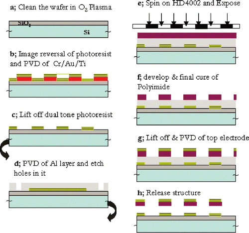
Figure 12. Optical image of bottom electrode and etched post holes.
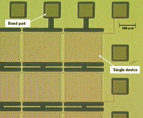
Figure 13. Cross-sectional SEM of polyimide rulings before (a) and after cure (b).
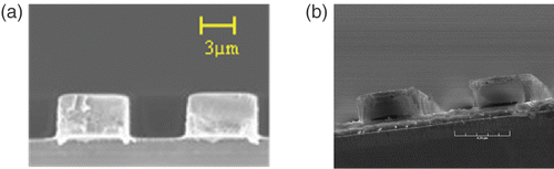
Figure 14. Top down SEM of the edge of single device after release.