Figures & data
Figure 1. (a) Four CNTFETs fabricated with four different metal interdigited electrodes (each colour corresponds to a different metal): in the inset, the carbon nanotubes chains connecting the two electrodes. On the right hand side, the transfer characteristic (source/drain current as a function of the gate voltage) of each transistor in air. (b) Change of the transfer characteristic of the four transistors as a consequence of the exposition to a particular gas (in the inset, the gas molecules that interact with the transistor): the four transfer characteristics change in a different way as a consequence of the various metal contacts (dashed line). Each gas gives a unique ‘signature’ in terms of IDS variation over the four transistors.
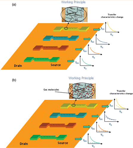
Figure 2. SEM picture of a CNT mat dispersed on a substrate after having been sonicated for three hours and centrifuged at 3000 rpm (2 times 10 minutes).
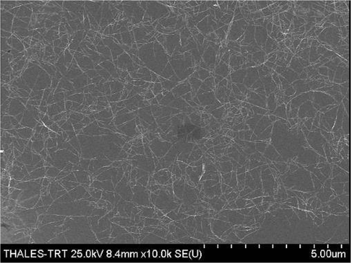
Figure 3. Left-hand side: SEM image of interdigited CNT transistors, Right-hand side: AFM detail of carbon nanotubes random network between two electrodes.
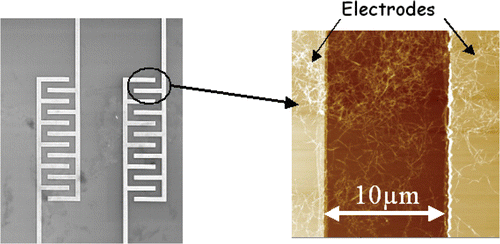
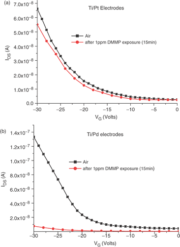
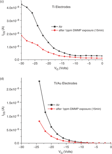
Figure 4. (a)–(d). Transfer characteristics change for the different metal electrodes after exposure to 1ppm of DMMP (VDS = 1V).