Figures & data
Figure 1. FG FET chip with 8 floating-gate PMOS transistors. (a) Chip surface showing the 8 recording FG transistors. (b) Cross section of the FG FET.
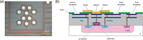
Figure 2. (a) Measurement principle of the FG FET in common source mode; (b) Photograph of the flow cell set-up.
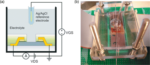
Figure 3. Fluorescent imaging of the presence of amine groups on the surface of different substrates. The arrows indicate the direction in which the relative fluorescence was monitored. (a) and (b): relative fluorescence of the amine groups on the APTES surface. (c) and (d): relative fluorescence image of the amine groups on the PLL surface.
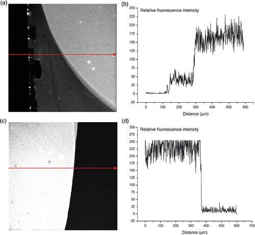
Figure 4. Fluorescent imaging of the adsorption of Alexa555 labelled DNA on different surfaces. The arrows indicate the direction in which the relative fluorescence was monitored. (a) and (b): relative fluorescence of DNA on the control surface with hydroxyl groups. (c) and (d): relative fluorescence of DNA on the APTES surface. (e) and (f): relative fluorescence of DNA on the PLL surface.
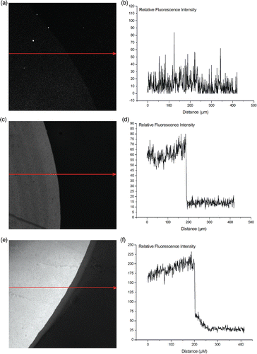
Figure 5. QCM monitoring of DNA hybridisation in buffers with different salt concentrations for the 3 above presented surfaces and for different target DNA concentrations: PLL layers are represented by the full line, APTES by the striped line, and the hydroxyl surface with the dotted line. All buffers were 10 mM phoshate buffers, pH7. The DNA hybridisation was allowed for 30 min. Regeneration of the hybridised DNA was performed with 2.5 mM HCl for 5 min.
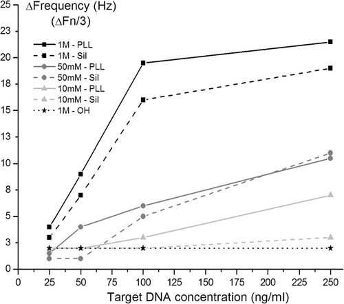
Figure 6. pH response of the Ta2O5 FG FET device in flow conditions. The bias applied ont the transistors were V DS = V GS = −1 V.
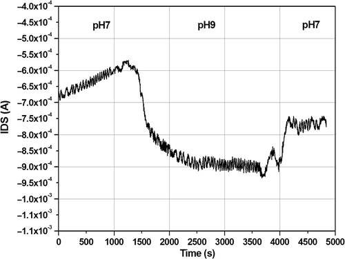
Figure 7. Adsorption of probe DNA (2.5 µM) in 10 mM phosphate buffer, pH7 on the surface of the FG FET. The biases are V DS = −2 V and V GS = −1.5 V. DNA was injected with a micropipette, rinsing was done by peristaltic pumping. The I DS shift caused by DNA addition is relatively large (∼50 µA).
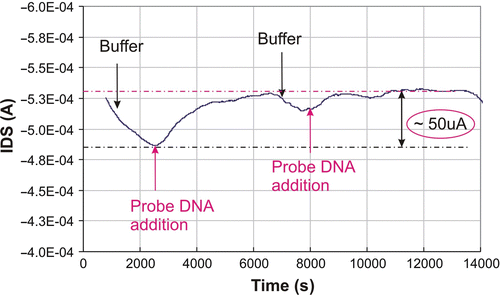
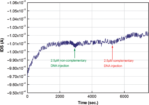
Figure 8. Hybridisation response after injection of a mixture of 2.5 µM complementary target DNA on the surface. Injection of noncomplementary DNA did not show a significant response in the channel of the transistor. The hybridisation buffer was a 10 mM phosphate buffer, containing 50 mM NaCl. The bias was V DS = −2 V and V GS = −1.5 V.