
Figures & data
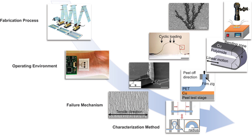
Figure 1. Overview of failure of flexible electronic devices from perspective of failure mode, characterization methods, fabrication process and operating environment. Strength failure: Adapted with permission. Copyright 2010, Elsevier BV [Citation40]. Interfacial failure: Adapted with permission. Copyright 2014, Elsevier BV [Citation41]. Fatigue failure: Adapted with permission. Copyright 2021, Wiley-VCH Verlag [Citation42]. Electrical failure: Reproduced with permission. Copyright 2022, American chemical Society [Citation43]. Bending strength test: Adapted with permission. Copyright 2018, Elsevier BV [Citation44]. Peel-off test. Adapted with permission. Copyright 2018, Elsevier BV [Citation44]. Laser-induced interfacial spallation. Adapted with permission. Copyright 2020, American chemical Society [Citation45]. Bending fatigue test. Adapted with permission. Copyright 2013, Elsevier BV [Citation46]. Tensile fatigue test. Adapted with permission. Copyright 2022, Nature Publishing group [Citation47]. Electromigration test. Adapted with permission. Copyright 2019, Springer Verlag [Citation48].
![Figure 1. Overview of failure of flexible electronic devices from perspective of failure mode, characterization methods, fabrication process and operating environment. Strength failure: Adapted with permission. Copyright 2010, Elsevier BV [Citation40]. Interfacial failure: Adapted with permission. Copyright 2014, Elsevier BV [Citation41]. Fatigue failure: Adapted with permission. Copyright 2021, Wiley-VCH Verlag [Citation42]. Electrical failure: Reproduced with permission. Copyright 2022, American chemical Society [Citation43]. Bending strength test: Adapted with permission. Copyright 2018, Elsevier BV [Citation44]. Peel-off test. Adapted with permission. Copyright 2018, Elsevier BV [Citation44]. Laser-induced interfacial spallation. Adapted with permission. Copyright 2020, American chemical Society [Citation45]. Bending fatigue test. Adapted with permission. Copyright 2013, Elsevier BV [Citation46]. Tensile fatigue test. Adapted with permission. Copyright 2022, Nature Publishing group [Citation47]. Electromigration test. Adapted with permission. Copyright 2019, Springer Verlag [Citation48].](/cms/asset/2c9d8bbd-8220-47da-a0bf-f760e7ecbd96/tsnm_a_2261775_f0001_c.jpg)
Figure 2. Schematic illustration of representative fabrication process for flexible electronic devices. (a) Photolithography process. Adapted with permission. Copyright 2016, Elsevier BV [Citation49]. (b) roll-to-roll printing. Reproduced with permission. Copyright 2018, American chemical Society [Citation50]. (c) deterministic assembly. Adapted with permission. Copyright 2021, Wiley-VCH Verlag [Citation51]. (d) inkjet printing process. Adapted with permission. Copyright 2018, American chemical Society [Citation52]. (e) mechanically guided 3D assembly of a resistive vibration sensor. Adapted with permission. Copyright 2021, Wiley-VCH Verlag [Citation42]. (f) encapsulation of a flexible microfluidic electronic system. Adapted with permission. Copyright 2014, American Association for the Advancement of Science [Citation53].
![Figure 2. Schematic illustration of representative fabrication process for flexible electronic devices. (a) Photolithography process. Adapted with permission. Copyright 2016, Elsevier BV [Citation49]. (b) roll-to-roll printing. Reproduced with permission. Copyright 2018, American chemical Society [Citation50]. (c) deterministic assembly. Adapted with permission. Copyright 2021, Wiley-VCH Verlag [Citation51]. (d) inkjet printing process. Adapted with permission. Copyright 2018, American chemical Society [Citation52]. (e) mechanically guided 3D assembly of a resistive vibration sensor. Adapted with permission. Copyright 2021, Wiley-VCH Verlag [Citation42]. (f) encapsulation of a flexible microfluidic electronic system. Adapted with permission. Copyright 2014, American Association for the Advancement of Science [Citation53].](/cms/asset/91b28536-bd97-44a2-9240-3c1d67b0e5c4/tsnm_a_2261775_f0002_c.jpg)
Figure 3. Operating environments of flexible electronic devices and their influencing factors. (a) Epidermal electronics. 1) flexible sensor arrays that can be used for pressure monitoring on human surfaces. Reproduced with permission. Copyright 2016, Nature Publishing group [Citation60]. 2) 3D-printed soft neural probe with nine channels by the conducting polymer ink and the PDMS ink. Reproduced with permission. Copyright 2020, Nature Publishing group [Citation61]. 3) Fractal device structure of the EEG measurement system, where the left image represents the device cascade on the auricle and mastoid, and the right image represents the amplified interconnections. Adapted with permission. Copyright 2015, Proceedings of the National Academy of Sciences [Citation62]. (b) implantable devices. 1) wireless biodegradable sensor wrapped around the femoral artery and secured with sutures. Adapted with permission. Copyright 2019, Nature Publishing group [Citation18]. 2) Implanted pressure sensor in front of the eye model. 3) wireless implanted pressure sensor with an external coil in front of the eye model. Reproduced with permission. Copyright 2008, IEEE [Citation63]. (c) textile-based devices. 1) Solid-state textile-based micro-supercapacitors. 2) the scanning electron microscopy (SEM) image of a solid-state textile- based micro-supercapacitors. Adapted with permission. Copyright 2016, Wiley-VCH Verlag [Citation19]. 3) textile-based pressure sensor. 4) LEDs lit by a DC source through knotted textile conductive circuits. Reproduced with permission. Copyright 2017, Wiley-VCH Verlag [Citation64]. (d) flexible electronic devices in engineering applications. 1) flexible skin for Boundary layer state measurement and flight Attitude Identification on unmanned aerial vehicle (UAV). Reproduced with permission. Copyright 2023, IOP Publishing [Citation13]. 2) schematic diagram of the UAV equipped with smart sensing skin for sensing wind pressure. Adapted with permission. Copyright 2020, Springer Verlag [Citation65].
![Figure 3. Operating environments of flexible electronic devices and their influencing factors. (a) Epidermal electronics. 1) flexible sensor arrays that can be used for pressure monitoring on human surfaces. Reproduced with permission. Copyright 2016, Nature Publishing group [Citation60]. 2) 3D-printed soft neural probe with nine channels by the conducting polymer ink and the PDMS ink. Reproduced with permission. Copyright 2020, Nature Publishing group [Citation61]. 3) Fractal device structure of the EEG measurement system, where the left image represents the device cascade on the auricle and mastoid, and the right image represents the amplified interconnections. Adapted with permission. Copyright 2015, Proceedings of the National Academy of Sciences [Citation62]. (b) implantable devices. 1) wireless biodegradable sensor wrapped around the femoral artery and secured with sutures. Adapted with permission. Copyright 2019, Nature Publishing group [Citation18]. 2) Implanted pressure sensor in front of the eye model. 3) wireless implanted pressure sensor with an external coil in front of the eye model. Reproduced with permission. Copyright 2008, IEEE [Citation63]. (c) textile-based devices. 1) Solid-state textile-based micro-supercapacitors. 2) the scanning electron microscopy (SEM) image of a solid-state textile- based micro-supercapacitors. Adapted with permission. Copyright 2016, Wiley-VCH Verlag [Citation19]. 3) textile-based pressure sensor. 4) LEDs lit by a DC source through knotted textile conductive circuits. Reproduced with permission. Copyright 2017, Wiley-VCH Verlag [Citation64]. (d) flexible electronic devices in engineering applications. 1) flexible skin for Boundary layer state measurement and flight Attitude Identification on unmanned aerial vehicle (UAV). Reproduced with permission. Copyright 2023, IOP Publishing [Citation13]. 2) schematic diagram of the UAV equipped with smart sensing skin for sensing wind pressure. Adapted with permission. Copyright 2020, Springer Verlag [Citation65].](/cms/asset/3507da6f-d7c5-4a54-b77d-235db2897830/tsnm_a_2261775_f0003_c.jpg)
Figure 4. Strength failure mechanisms. (a) illustration of the three stages of brittle film fragmentation under uniaxial loading; the insets show the progression of cracks of a 20 nm thick SiOx coating on a 12 μm thick PET substrate. Adapted with permission. Copyright 2002, Elsevier BV [Citation109]. (b) Demonstration of the failure of a flexible accelerometer upon impact. Adapted with permission. Copyright 2014, Elsevier BV [Citation113]. (c) analytical model of stretchable electronic devices with viscoelastic packages and soft substrates subjected to impact loads on the surface of human skin. Adapted with permission. Copyright 2016, ASME [Citation114]. (d) flexible microfluidic electronic systems under stretch and twist configurations. Adapted with permission. Copyright 2014, American Association for the Advancement of Science [Citation53]. (e) left, schematic illustration of a flexible sensor with a non-bonded interface, exhibiting a notable mechanical mismatch between the layers. Right, SEM image of the sensor in its bent state, highlighting stable bonding between the microcones and the dielectric layers. Adapted with permission. Copyright 2022, Nature Publishing group [Citation115]. (f) left, SEM image of the cross-section of an organic–inorganic multilayer permeation barrier. Right, the evolution of defects: beginning as pin-holes, escalating to channel cracks, and culminating in the delamination of the oxide-organic interface. Adapted with permission. Copyright 2010, Elsevier BV [Citation116].
![Figure 4. Strength failure mechanisms. (a) illustration of the three stages of brittle film fragmentation under uniaxial loading; the insets show the progression of cracks of a 20 nm thick SiOx coating on a 12 μm thick PET substrate. Adapted with permission. Copyright 2002, Elsevier BV [Citation109]. (b) Demonstration of the failure of a flexible accelerometer upon impact. Adapted with permission. Copyright 2014, Elsevier BV [Citation113]. (c) analytical model of stretchable electronic devices with viscoelastic packages and soft substrates subjected to impact loads on the surface of human skin. Adapted with permission. Copyright 2016, ASME [Citation114]. (d) flexible microfluidic electronic systems under stretch and twist configurations. Adapted with permission. Copyright 2014, American Association for the Advancement of Science [Citation53]. (e) left, schematic illustration of a flexible sensor with a non-bonded interface, exhibiting a notable mechanical mismatch between the layers. Right, SEM image of the sensor in its bent state, highlighting stable bonding between the microcones and the dielectric layers. Adapted with permission. Copyright 2022, Nature Publishing group [Citation115]. (f) left, SEM image of the cross-section of an organic–inorganic multilayer permeation barrier. Right, the evolution of defects: beginning as pin-holes, escalating to channel cracks, and culminating in the delamination of the oxide-organic interface. Adapted with permission. Copyright 2010, Elsevier BV [Citation116].](/cms/asset/fe06cc86-c2bb-4636-9b85-0f29e00dc82b/tsnm_a_2261775_f0004_c.jpg)
Table 1. Characterization methods of strength failure.
Figure 5. Characterization methods for strength failure. (a) SEM images of Mo films of varying thickness - (I) 500 nm, (II) 250 nm, (III) 70 nm, and (Ⅳ) 40 nm - on PI substrates after the application of a 12% strain. Adapted with permission. Copyright 2017, Elsevier BV [Citation130]. (b) the falling ball test, employed to evaluate the reliability of pressure stress concentrations in flexible displays. Left, a fully supported sample backed by a solid steel block. Right, a partially supported sample propped on two rollers. Reproduced with permission. Copyright 2008, IEEE [Citation176]. (c) static bending test of the CIF assembly, utilizing bending rods of varied radii. Adapted with permission. Copyright 2016, IEEE [Citation177]. (d) three-point static bending test. Reproduced with permission. Copyright 2016, IEEE [Citation177]. (e) the lab-made bending test machine and outer/inner bending test experiments. Reproduced with permission. Copyright 2014, Elsevier BV [Citation178]. (f) optical device for strain measurement on the surface of a curved film. Adapted with permission. Copyright 2021, Wiley-VCH Verlag [Citation179].
![Figure 5. Characterization methods for strength failure. (a) SEM images of Mo films of varying thickness - (I) 500 nm, (II) 250 nm, (III) 70 nm, and (Ⅳ) 40 nm - on PI substrates after the application of a 12% strain. Adapted with permission. Copyright 2017, Elsevier BV [Citation130]. (b) the falling ball test, employed to evaluate the reliability of pressure stress concentrations in flexible displays. Left, a fully supported sample backed by a solid steel block. Right, a partially supported sample propped on two rollers. Reproduced with permission. Copyright 2008, IEEE [Citation176]. (c) static bending test of the CIF assembly, utilizing bending rods of varied radii. Adapted with permission. Copyright 2016, IEEE [Citation177]. (d) three-point static bending test. Reproduced with permission. Copyright 2016, IEEE [Citation177]. (e) the lab-made bending test machine and outer/inner bending test experiments. Reproduced with permission. Copyright 2014, Elsevier BV [Citation178]. (f) optical device for strain measurement on the surface of a curved film. Adapted with permission. Copyright 2021, Wiley-VCH Verlag [Citation179].](/cms/asset/0e3f123d-df2c-4acb-8cc0-1da7af65e52f/tsnm_a_2261775_f0005_c.jpg)
Figure 6. Interfacial failure mechanisms alongside their characterization methods. (a) in situ SEM images capturing the progressive sliding at the interface of a horseshoe-shaped copper interconnect deposited on PDMS, stretched sequentially to 30%, 50%, and 100%. Adapted with permission. Copyright 2011, IOP Publishing [Citation209]. (b) delamination between PI layers of prototype stretchable interconnect. (1) SEM image of a bonded sample where PI has been printed once on the top and bottom layers of encapsulated silver, following cooling from curing temperature to ambient temperature. (2) SEM image of a delaminated sample with PI printed three times on the top and bottom layers of encapsulated silver, following cooling from curing temperature to ambient temperature. (3) optical image of a printed interconnect, showcasing variable silver width and PI thickness after cooling from curing temperature to room temperature. Adapted with permission. Copyright 2021, Elsevier BV [Citation210]. (c) the 3M tape adhesion test on the Cu/PET interface, following plasma treatments for durations of 0 min (left) and 7 min (Right). Reproduced with permission. Copyright 2017, Elsevier BV [Citation44]. (d) Scotch tape adhesion test for an al feature on a magazine paper substrate. Reproduced with permission. Copyright 2012, American chemical Society [Citation211]. (e) a peel test device integrated with a camera for examining the local geometry of the delamination front. Adapted with permission. Copyright 2010, IOP Publishing [Citation209]. (f) schematic illustration of T-peel test on Cu/PET flexible substrate. Adapted with permission. Copyright 2017, Elsevier BV [Citation44]. (g) schematic illustration of the laser-induced interplanar sputtering (LIIS) process, employed to facilitate the delamination of PI film from its substrate. Adapted with permission. Copyright 2020, American chemical Society [Citation45].
![Figure 6. Interfacial failure mechanisms alongside their characterization methods. (a) in situ SEM images capturing the progressive sliding at the interface of a horseshoe-shaped copper interconnect deposited on PDMS, stretched sequentially to 30%, 50%, and 100%. Adapted with permission. Copyright 2011, IOP Publishing [Citation209]. (b) delamination between PI layers of prototype stretchable interconnect. (1) SEM image of a bonded sample where PI has been printed once on the top and bottom layers of encapsulated silver, following cooling from curing temperature to ambient temperature. (2) SEM image of a delaminated sample with PI printed three times on the top and bottom layers of encapsulated silver, following cooling from curing temperature to ambient temperature. (3) optical image of a printed interconnect, showcasing variable silver width and PI thickness after cooling from curing temperature to room temperature. Adapted with permission. Copyright 2021, Elsevier BV [Citation210]. (c) the 3M tape adhesion test on the Cu/PET interface, following plasma treatments for durations of 0 min (left) and 7 min (Right). Reproduced with permission. Copyright 2017, Elsevier BV [Citation44]. (d) Scotch tape adhesion test for an al feature on a magazine paper substrate. Reproduced with permission. Copyright 2012, American chemical Society [Citation211]. (e) a peel test device integrated with a camera for examining the local geometry of the delamination front. Adapted with permission. Copyright 2010, IOP Publishing [Citation209]. (f) schematic illustration of T-peel test on Cu/PET flexible substrate. Adapted with permission. Copyright 2017, Elsevier BV [Citation44]. (g) schematic illustration of the laser-induced interplanar sputtering (LIIS) process, employed to facilitate the delamination of PI film from its substrate. Adapted with permission. Copyright 2020, American chemical Society [Citation45].](/cms/asset/80c681aa-7c4c-40c1-bd26-f0dfbfbf6003/tsnm_a_2261775_f0006_c.jpg)
Table 2. Characterization methods of interfacial failure.
Figure 7. Fatigue failure mechanisms. (a) resistance changes of serpentine interconnects under cyclic loading with different tensile strains. Adapted with permission. Copyright 2021, Wiley-VCH Verlag [Citation264]. (b) resistance change of flexible NiCr-based strain gauges under cyclic bending deformation. (1) resistance response illustrates an upward shift in the baseline correlating with increased peak resistance; (2) SEM images of cracks in an unconstrained position; (3) schematic illustration for the evolution of cracks, starting from initial unconstrained state, proceeding through opening during bending, and culminating in a state of partial closure after stress relief. Adapted with permission. Copyright 2022, Elsevier BV [Citation265].
![Figure 7. Fatigue failure mechanisms. (a) resistance changes of serpentine interconnects under cyclic loading with different tensile strains. Adapted with permission. Copyright 2021, Wiley-VCH Verlag [Citation264]. (b) resistance change of flexible NiCr-based strain gauges under cyclic bending deformation. (1) resistance response illustrates an upward shift in the baseline correlating with increased peak resistance; (2) SEM images of cracks in an unconstrained position; (3) schematic illustration for the evolution of cracks, starting from initial unconstrained state, proceeding through opening during bending, and culminating in a state of partial closure after stress relief. Adapted with permission. Copyright 2022, Elsevier BV [Citation265].](/cms/asset/7eeb7e27-040f-46a3-82b7-6a6bd4aadaea/tsnm_a_2261775_f0007_c.jpg)
Table 3. Characterization methods of fatigue failure.
Figure 8. Characterization methods of fatigue failure. (a)-(e).Schematic illustrations and devices of the bending test method for fatigue endurance. (a) free arc bending test. Reproduced with permission. Copyright 2021, Elsevier BV [Citation294]. (b) variable radius bending test. Reproduced with permission. Copyright 2017, Nature Publishing group [Citation141]. (c) sliding plate test. Adapted with permission. Copyright 2013, Elsevier BV [Citation46]. (d) variable angle test for unidirectional bending. Adapted with permission. Copyright 2016, IEEE [Citation295]. (e) variable angle test for bidirectional bending. Reproduced with permission. Copyright 2011, IEEE [Citation267]. (f) Biaxial cyclic tensile testing system. Adapted with permission. Copyright 2022, American chemical Society [Citation296]. (g) schematic illustration of cyclic rubbing test. Adapted with permission. Copyright 2022, Nature Publishing group [Citation115].
![Figure 8. Characterization methods of fatigue failure. (a)-(e).Schematic illustrations and devices of the bending test method for fatigue endurance. (a) free arc bending test. Reproduced with permission. Copyright 2021, Elsevier BV [Citation294]. (b) variable radius bending test. Reproduced with permission. Copyright 2017, Nature Publishing group [Citation141]. (c) sliding plate test. Adapted with permission. Copyright 2013, Elsevier BV [Citation46]. (d) variable angle test for unidirectional bending. Adapted with permission. Copyright 2016, IEEE [Citation295]. (e) variable angle test for bidirectional bending. Reproduced with permission. Copyright 2011, IEEE [Citation267]. (f) Biaxial cyclic tensile testing system. Adapted with permission. Copyright 2022, American chemical Society [Citation296]. (g) schematic illustration of cyclic rubbing test. Adapted with permission. Copyright 2022, Nature Publishing group [Citation115].](/cms/asset/4996c98c-86aa-4abf-8b85-24eef1566109/tsnm_a_2261775_f0008_c.jpg)
Figure 9. Electrical failure mechanisms and characterization methods. (a) microstructural illustrations of silver-printed interconnects pre-failure (I) and post open-circuit failure (II), along with a SEM image at the cathode (III). Adapted with permission. Copyright 2019, Springer Verlag [Citation48]. (b) Electrothermal coupling failure mechanism of stretchable thin-film conductors: (I) SEM image of an initially planar electrode (inset) displaying random intrinsic nano-cracks on the electrode; (II) SEM image of the fracture region (inset) post failure, along with a SEM image presenting dispersed metal particles within the crack, induced by electrical discharge. Adapted with permission. Copyright 2022, American chemical Society [Citation312]. (c) (1) TEM images of the lithiation process of spherical silicon particles: expansion and cracking of the outer layer of the particles occurs. Adapted with permission. Copyright 2012, American chemical Society [Citation315]. (2) SEM images of nanowires in their initial and lithiated expanded states. Adapted with permission. Copyright 2015, Nature Publishing group [Citation316]. (d) (1) schematic diagram of the experimental setup for IR measurement during electromigration tests. (2) schematic representation of a dog-bone pattern structure of Ag interconnects. (3) SEM image of the microstructure of as-sintered interconnects. Adapted with permission. Copyright 2019, Springer Verlag [Citation48]. (e) schematic illustrations (1) and images (2) of the electrothermal coupling failure process of stretchable thin-film conductors. Adapted with permission. Copyright 2019, Springer Verlag [Citation312].
![Figure 9. Electrical failure mechanisms and characterization methods. (a) microstructural illustrations of silver-printed interconnects pre-failure (I) and post open-circuit failure (II), along with a SEM image at the cathode (III). Adapted with permission. Copyright 2019, Springer Verlag [Citation48]. (b) Electrothermal coupling failure mechanism of stretchable thin-film conductors: (I) SEM image of an initially planar electrode (inset) displaying random intrinsic nano-cracks on the electrode; (II) SEM image of the fracture region (inset) post failure, along with a SEM image presenting dispersed metal particles within the crack, induced by electrical discharge. Adapted with permission. Copyright 2022, American chemical Society [Citation312]. (c) (1) TEM images of the lithiation process of spherical silicon particles: expansion and cracking of the outer layer of the particles occurs. Adapted with permission. Copyright 2012, American chemical Society [Citation315]. (2) SEM images of nanowires in their initial and lithiated expanded states. Adapted with permission. Copyright 2015, Nature Publishing group [Citation316]. (d) (1) schematic diagram of the experimental setup for IR measurement during electromigration tests. (2) schematic representation of a dog-bone pattern structure of Ag interconnects. (3) SEM image of the microstructure of as-sintered interconnects. Adapted with permission. Copyright 2019, Springer Verlag [Citation48]. (e) schematic illustrations (1) and images (2) of the electrothermal coupling failure process of stretchable thin-film conductors. Adapted with permission. Copyright 2019, Springer Verlag [Citation312].](/cms/asset/cc44386e-1d50-4a7b-9d31-3fb792ac414a/tsnm_a_2261775_f0009_c.jpg)
Table 4. Characterization methods of electrical failure.
Table 5. Comparison among the four failure modes.