Figures & data
Figure 1. The test rig for recording a signal of AE elastic waves from IGBT transistor switching.
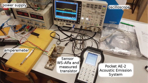
Figure 2. Dimensions of the Hsu-Nilsen calibration head (Bejger Citation2012; ASTM Citation2015).
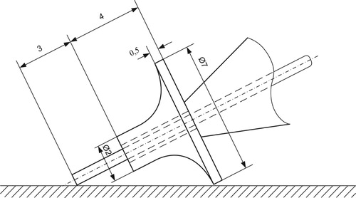
Figure 3. Scheme of experimental rig used in switching transistor Q1 acoustic emission tests.
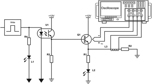
Figure 4. The signal of radiated AE elastic wave during the IGBT transistor switching, (left – time-voltage signal, right – amplitude-time signal). The measurements were made with a Pocket AE2, MISTRAS-made analyser (Physical Acoustic Corp.).
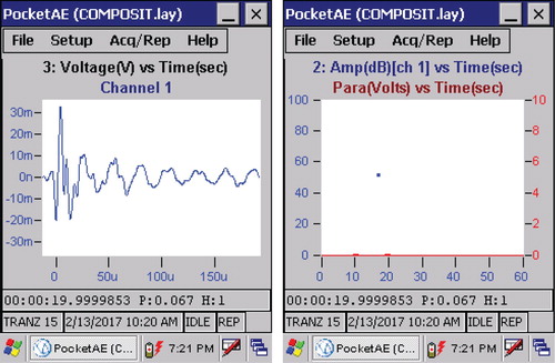
Figure 5. The source signal of the AE elastic wave (left) and its frequency analysis (right).
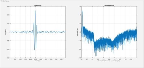
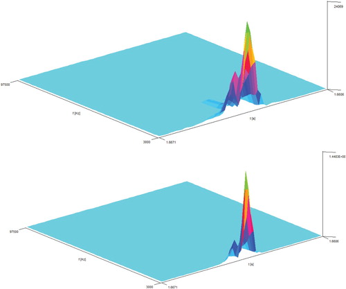
Figure 6. A wavelet analysis of acoustic emission from switching an IGBT transistor.
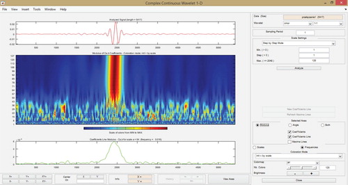
Figure 7. The infrared camera display showing the temperature of tested transistor.
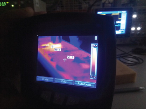
Figure 8. Results of wavelet analysis obtained at 80°C (raw signal from the AE sensor on the left, wavelet analysis result applied to the signal on the right).
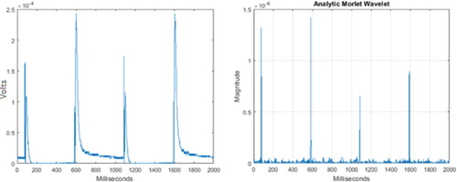
Figure 9. Results of wavelet analysis obtained at 96°C (raw signal from the AE sensor on the left, wavelet analysis result applied to the signal on the right).
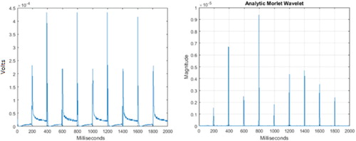
Figure 10. Analysis of the power spectral density of the AE signal during bipolar transistor switch.