Figures & data
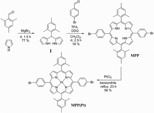
Scheme 1. Synthesis of MPP(Pt).
Scheme 2. Suzuki–Miyaura polymerisation of 2, 3 and MPP(Pt) to form PF-MPP(Pt).
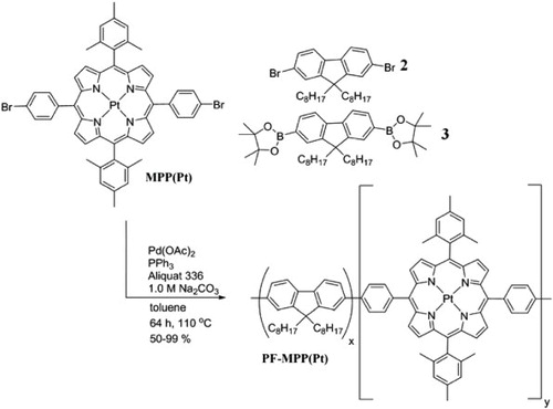
Figure 1. H1 NMR spectra in CDCl3 of PF-MPP(Pt) containing 0.5% (P1, purple, top), 1.0% (P2, cyan, second from top), 2.0% (P3, green, second from bottom) and 5.0% (P4, maroon, bottom) w/w of MPP(Pt). PF observed peaks (top right) were set to the same level. Peaks corresponding to porpyhin protons are shown in dotted boxes.
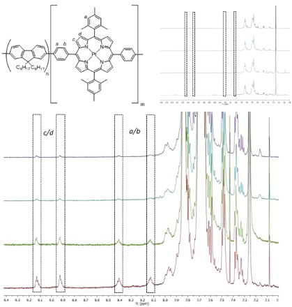
Table 1. Synthetic results of polymerisation.
Figure 2. HOMO and LUMO levels of PF-MPP(Pt).
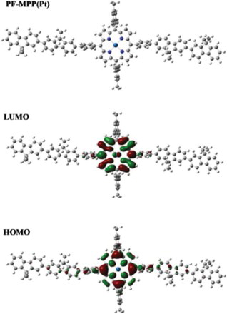
Figure 3. (a) Chemical structure of the PFO-MPP(Pt) copolymers with different MPP(Pt) loading: 0.5% for P1, 1% for P2, 2% for P3 and 5% for P4. (b) Normalised absorption spectra of the copolymers film on fused silica glass. The inset shows MPP(Pt) absorption features, the curves are stacked with Y-offset following the increase in the MPP(Pt) content. (c) Normalised PL spectra of the copolymer films. The ‘*’ indicates the monochromator second-order transmission of the excitation wavelength. (d) PL time decay taken at the most intense peak emission wavelength of the MPP(Pt) (665 nm) following excitation at 371 nm.
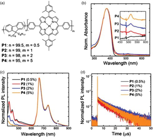
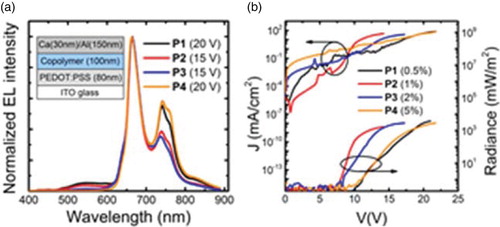
Figure 4. (a) Normalised EL spectra for the copolymers. The LED structure is reported. (b) LED characteristics: current density and radiance versus voltage. The active layer thickness is ∼100 nm and the device area is 3.5 mm2.