
Figures & data
Figure 1. (a) Typical TEM micrograph showing the UFG microstructure produced by phase reversion transformation, (b) EBSD image. The black lines denote random GBs and the colored lines represent coincident-site lattice boundaries, of which the Σ3 TBs are represented by red lines, (c) distribution of twin thickness, (d) distribution of GB misorientation angles.
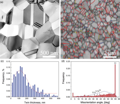
Figure 2 (a) Typical tensile true stress–strain curves for UFG and CG 304 L SSs at a quasi-static strain rate of 5 × 10⁻⁴ s−1 and RT. The inset is engineering stress–strain curves, (b) excellent strength–ductility combination of the current ideal UFG SS in comparison with other 304 L SSs (with Ni content of 10∼12%).
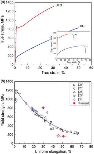
Figure 3. Typical TEM micrographs showing the microstructures and defects in ultrafine austenitic grains after ∼28% tensile strain: (a) overview of the microstructure, (b) defect structure in a 520 nm grain, (c) a 400 × 570 nm grain with an annealing twin, (d) a 500 × 700 nm grain with two nanotwins. The corresponding SAD patterns with [011] zone axis are shown in the insets. The insets denoted by capital letters A and B are enlarged from the corresponding white frame regions, which reveal different slip planes activated in different regions.
![Figure 3. Typical TEM micrographs showing the microstructures and defects in ultrafine austenitic grains after ∼28% tensile strain: (a) overview of the microstructure, (b) defect structure in a 520 nm grain, (c) a 400 × 570 nm grain with an annealing twin, (d) a 500 × 700 nm grain with two nanotwins. The corresponding SAD patterns with [011] zone axis are shown in the insets. The insets denoted by capital letters A and B are enlarged from the corresponding white frame regions, which reveal different slip planes activated in different regions.](/cms/asset/7c85ed44-bf4d-4201-9e7c-ee5f66b7d704/tmrl_a_968680_f0003_c.jpg)
Figure 4. High density of SFs (indicated by arrows) formed inside nanotwin lamellae. The upper-right inset is corresponding SAD pattern with the [011] zone axis. The lower-left inset is an HRTEM image showing a stacking fault formed within a nanotwin.
![Figure 4. High density of SFs (indicated by arrows) formed inside nanotwin lamellae. The upper-right inset is corresponding SAD pattern with the [011] zone axis. The lower-left inset is an HRTEM image showing a stacking fault formed within a nanotwin.](/cms/asset/e790e110-ecaa-482b-ac69-8764c21f99d2/tmrl_a_968680_f0004_c.jpg)