Figures & data
Figure 1. (a) Resistivity, (b) carrier density and (c) carrier mobility as a function of In concentration. Squares and circles represent In-doped Si0.35Ge0.65 [6] and C + In co-doped Si0.35Ge0.65, respectively. In panel (b), un-bracketed and bracketed numbers are the electrically active fractions for In-doped Si0.35Ge0.65 [6] and C + In co-doped Si0.35Ge0.65, respectively.
![Figure 1. (a) Resistivity, (b) carrier density and (c) carrier mobility as a function of In concentration. Squares and circles represent In-doped Si0.35Ge0.65 [6] and C + In co-doped Si0.35Ge0.65, respectively. In panel (b), un-bracketed and bracketed numbers are the electrically active fractions for In-doped Si0.35Ge0.65 [6] and C + In co-doped Si0.35Ge0.65, respectively.](/cms/asset/2b02bb37-cb17-4451-b8e2-0e083187df21/tmrl_a_1169229_f0001_c.jpg)
Figure 2. The Fourier-transformed, k2-weighted EXAFS spectra as a function of radial distance for (a) the In-doped Si0.35Ge0.65 [6] and (b) C + In co-doped Si0.35Ge0.65 samples, respectively.
![Figure 2. The Fourier-transformed, k2-weighted EXAFS spectra as a function of radial distance for (a) the In-doped Si0.35Ge0.65 [6] and (b) C + In co-doped Si0.35Ge0.65 samples, respectively.](/cms/asset/2d4a0d23-4021-44db-9421-085c818f733a/tmrl_a_1169229_f0002_c.jpg)
Table 1. A summary of the quantified fractions (from Figure ) of In atoms in substitutional sites (S), metallic In (M), random lattice location (R) and substitutional sites pairing with C (C) of the In [6] and C + In-implanted Si0.35Ge0.65 samples.
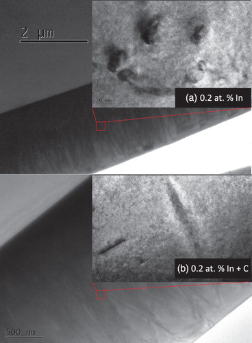
Figure 3. Cross-sectional TEM images for (a) 0.2 at% In doped Si0.35Ge0.65 and (b) 0.2 at% C + In co-doped Si0.35Ge0.65.