Figures & data
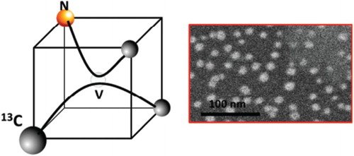
Figure 1. (a) Atomic structure of substitutional nitrogen and vacancy (NV) defect in <110> chain of diamond; and (b) NV defect in a diamond tetrahedron contained in (a/2,a/2,a/2) diamond unit cell, where one of the carbon can be replaced by magnetic isotope 13C.
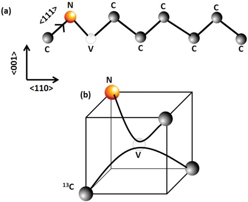
Figure 2. High-resolution SEM micrographs of nanodiamonds from pure undoped samples: (a) nanodiamonds with inset at a higher magnification; (b) mechanism of nanodiamond formation from Q-Carbon; (c) formation of nanodiamonds during initial stages and EBSD pattern (from red dot), showing characteristic diamond Kikuchi pattern; and (d) microdiamonds covering the entire area with inset showing twins whose density is controlled by quenching rates.
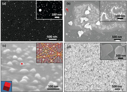
Figure 3. High-resolution SEM micrographs of nanodiamonds and microdiamonds from N-doped samples: (a) nanodiamonds with inset diamond EBSD Kikuchi pattern and orientation (from red dot), it also shows flat nanodiamond nanoplates (indicated as 1) and perpendicular nanoplates of diamond (indicated as 2); (b) microdiamonds from N-doped samples containing twins; and (c) nanoneedles and microneedles from N-doped sample with inset characteristic diamond pattern and orientation from the spot indicated.
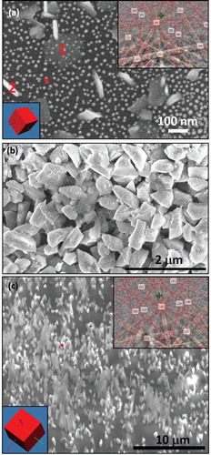
Figure 4. Raman spectra from N-doped samples: (a) different N-doping by varying nitrogen pressure after laser treatment, including undoped control sample; (b) different N-doping by changing the ion flux after laser treatment, including the control (before laser annealing) sample; and (c) change in Raman shift, down shift due to size (nanorange) and upshift as a result of quenched-in stress.
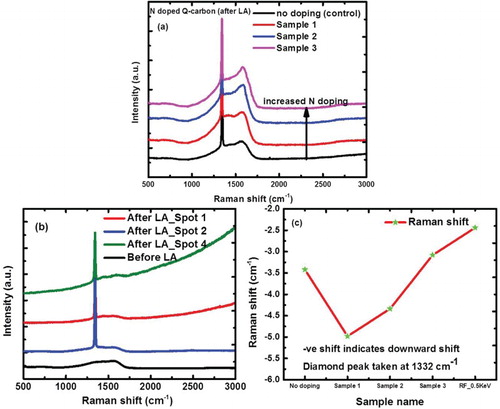
Figure 5. PL spectrum containing ZPL from NV− (637 nm) and NV0 (575 nm) defects. The inset (100× magnification) shows transitions from individual nanodiamonds when the sample is irradiated with 532 nm PL source.
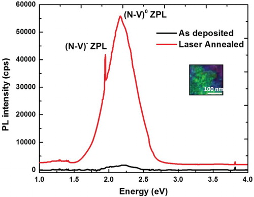
Figure 6. (a) Electrical pumping of NV centers using 14 mW laser power (532 nm excitation wavelength); (b) PL spectra of NV diamond in 0–21 V external electric field; and (c) optical and electrical pumping of NV centers using 532 nm laser.
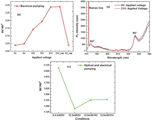
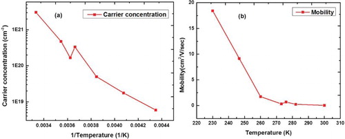
Figure 7. (a) Carrier concentration plotted as 1/T; and (b) Hall mobility as a function of T.