Figures & data
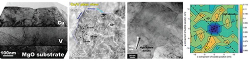
Figure 1. (a) Cross-sectional TEM micrograph of a Cu–V bilayer film deposited on an MgO substrate. (b) Corresponding diffraction pattern showing that the following crystallographic directions are parallel within the interface planes: Cu[110]||V[111]||MgO[110]. (c) Atomic structure of the interface showing that the interface plane is parallel to Cu(111) and V(110) planes. Interface misfit dislocations that contain an edge component and intersect the image plane are marked by red ‘⊥’ symbols. (d) Magnified image of the yellow dashed box in (c).
![Figure 1. (a) Cross-sectional TEM micrograph of a Cu–V bilayer film deposited on an MgO substrate. (b) Corresponding diffraction pattern showing that the following crystallographic directions are parallel within the interface planes: Cu[110]||V[111]||MgO[110]. (c) Atomic structure of the interface showing that the interface plane is parallel to Cu(111) and V(110) planes. Interface misfit dislocations that contain an edge component and intersect the image plane are marked by red ‘⊥’ symbols. (d) Magnified image of the yellow dashed box in (c).](/cms/asset/f3530ea0-255e-458a-9e69-fa2cf3c58f22/tmrl_a_1287132_f0001_c.jpg)
Figure 2. (a) Plan-view TEM image of an as-deposited Cu/V bilayer showing slip steps created at the Cu/V interface by threading dislocations. (b) Schematic diagram of the orientation of (111) glides planes in the Cu film relative to the Cu/V interface.
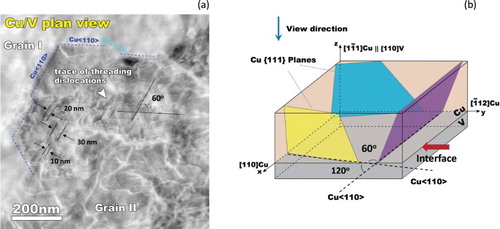
Figure 3. (a) Plan-view TEM image of helium implanted Cu/V foil, taken with under-focus of 400 nm. Helium bubbles appear to align preferentially at grain boundaries and along Cu⟨110⟩-type crystallographic directions. (b) Edges of He bubbles at the Cu/V interface imaged by high-resolution TEM, taken with under-focus of 200 nm.
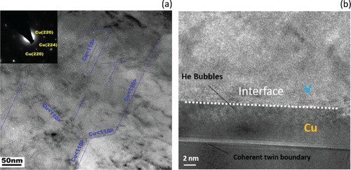
Figure 4. (a) Under-focused and (b) over-focused plan-view TEM micrographs of a He-implanted Cu/V bilayer, taken with defocusing of minus and plus 400 nm respectively. (c) An image generated by subtracting (b) from (a). The plot of the digitized He bubble positions obtained from (c) is given in (d). Bubble areas in (d) are exaggerated by a factor of five for clarity. The red circles illustrate regions that do not contain GBs decorated by He atoms. Bubbles drawn from these regions are used for the statistical analysis described in the text.
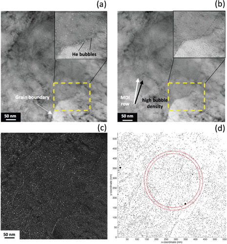
Figure 5: (a) Distribution of bubble radii. (b) Bubble pair distribution function as a function of distance between bubbles. (c) Bubble pair distribution function expressed in terms of the x- and y-positions of bubbles neighboring a central bubble.
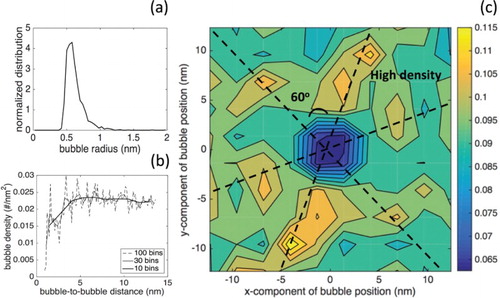
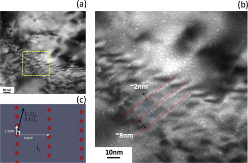
Figure 6. (a) Plan-view TEM image of aligned He bubbles, taken with under-focus of 400 nm; (b) magnified image of the yellow dashed box in (a); and (c) schematic diagram of MDIs at a Cu/V interface with KS orientation relationship.