
Figures & data
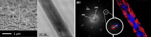
Figure 1. SEM images of Ge/In–Te NWs grown on different substrates and catalysed by 20 nm Au NPs: (a) top view on Si (001); (b) tilted view on Si (110).
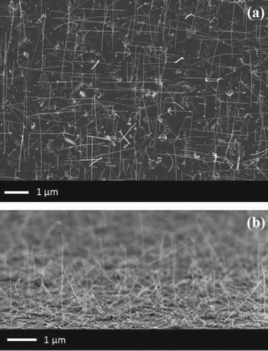
Figure 2. (a) Low magnification TEM image of a {001} oriented core–shell NW. (b) FFT of (a). (c) Map representing in false colours the region where the InTe (red) and Ge (blue) phases are observed. The map is colour-coded according to the FFT magnification reported as inset. (d) High magnification TEM and (e) zoomed HR-TEM of a second {001} oriented core–shell NW. (f) Measurements of the periodicity of the Moiré fringes formed by the superposition of the parallel sets of planes.
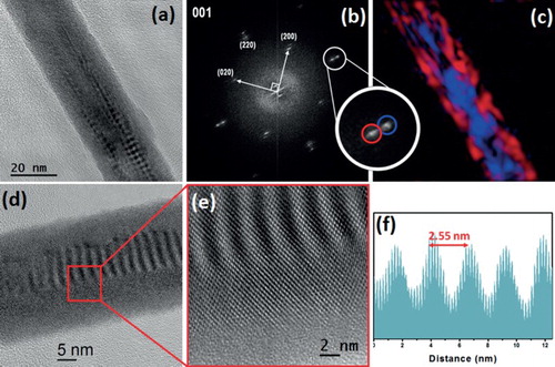
Figure 3. (a) STEM-HAADF image of a core–shell NW and its EDX map. The elemental maps of each atomic species are reported in (c)–(f), according to their labels (the markers correspond to 20 nm); the overall elemental map is shown in (b).
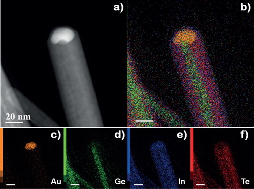
Figure 4. (a) Raman spectra obtained on an ensemble of as-grown NWs catalysed by 10 Au NPs on Si (001) (red solid line) and on 5 different single NWs transferred on a Si (111) substrate (black solid lines). Vertical dashed lines mark the frequencies of the modes related to InTe and Ge. (b) Raman spectrum of a representative single NW (open circles), with individual Lorentzian contributions deconvoluted (solid lines).
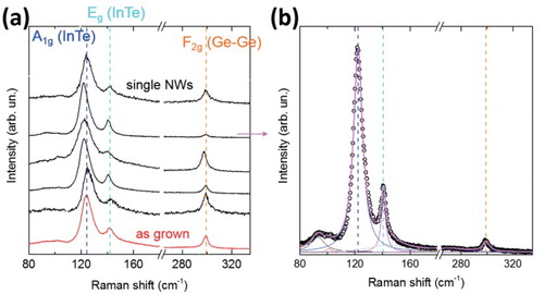
Figure 5. (a), (b) and (c) XRD Φ scans performed on samples with the same substrate size and NWs catalysed by 10, 20 and 50 nm Au NPs, respectively, showing the counts of plane [001] orientation of the NWs and their in-plane [110] orientation. (d) Some selected diffractograms obtained from a sample grown on Si (001) using 30 nm Au NPs. (e) Superposition for the samples grown on Si (001) using 10, 20, 30 and 50 nm Au NPs of the diffractograms obtained in front of the <110> direction (red) and at 45° from the <110> direction (blue).
![Figure 5. (a), (b) and (c) XRD Φ scans performed on samples with the same substrate size and NWs catalysed by 10, 20 and 50 nm Au NPs, respectively, showing the counts of plane [001] orientation of the NWs and their in-plane [110] orientation. (d) Some selected diffractograms obtained from a sample grown on Si (001) using 30 nm Au NPs. (e) Superposition for the samples grown on Si (001) using 10, 20, 30 and 50 nm Au NPs of the diffractograms obtained in front of the <110> direction (red) and at 45° from the <110> direction (blue).](/cms/asset/17519f6f-e7b3-4452-a0bb-4bb21f6aa7d2/tmrl_a_1384409_f0005_c.jpg)