Figures & data
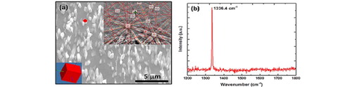
Table 1. Key properties of diamond and c-BN.
Figure 1. Gibbs free energy vs. temperature for graphite (Gg), liquid carbon (Gliq), and diamond (Gd).
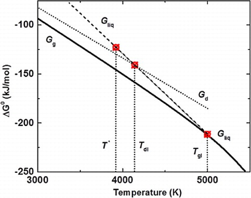
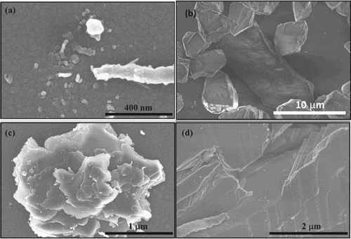
Figure 2. (a) Formation of Q-carbon and growth of diamond from Q-carbon, (b) large-area Q-carbon, (c) microcrystals of diamond, and (d) large-area single-crystal diamond film on (0001) sapphire.
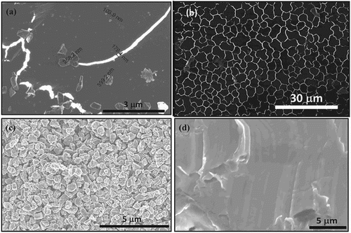
Figure 3. (a) Atomic structure of DCL, (b) subunit cell (D1), and (c) subunit cell (D2).
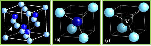
Table 2. Experimental and theoretical values of Young’s modulus (E), bulk modulus (B), Poisson’s ratio (υ), and shear modulus (µ) directly related to hardness.
Figure 4. (a) Topography of Q-carbon filaments formed on a diamond-like carbon (DLC) film. (b) Topography of a filament cross-section; markers indicate positions across the filament where indentation measurements are conducted. (c) Indentation curves measured on the Q-carbon filament. Blue and red lines are measurements performed on the Q-carbon filament and the surrounding DLC film, respectively. Numbers refer to positions identified in (b) [Citation9].
![Figure 4. (a) Topography of Q-carbon filaments formed on a diamond-like carbon (DLC) film. (b) Topography of a filament cross-section; markers indicate positions across the filament where indentation measurements are conducted. (c) Indentation curves measured on the Q-carbon filament. Blue and red lines are measurements performed on the Q-carbon filament and the surrounding DLC film, respectively. Numbers refer to positions identified in (b) [Citation9].](/cms/asset/88c8cb98-7204-45d6-8f79-011aed537351/tmrl_a_1458753_f0004_c.jpg)
Figure 5. The experimentally measured Young’s modulus of Q-carbon as 1702 ± 138 GPa, compared to 1015 ± 107 GPa for diamond and 350 ± 30 GPa for sapphire [Citation9].
![Figure 5. The experimentally measured Young’s modulus of Q-carbon as 1702 ± 138 GPa, compared to 1015 ± 107 GPa for diamond and 350 ± 30 GPa for sapphire [Citation9].](/cms/asset/07374574-cf3f-4749-821d-05f270ee84c2/tmrl_a_1458753_f0005_c.jpg)
Figure 6. M vs. H plots of Q-carbon at different temperatures (10, 50, 100, 200, and 300 K) showing ferromagnetic characteristics. The upper inset shows magnetic force microscope (MFM) image of Q-carbon at 300 K. The lower right inset shows the diamagnetic signal from as-deposited DLC and the lower left inset shows finite coercivity (∼100 Oe) at 100 K.
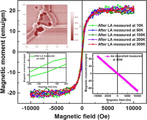
Figure 7. (a) I-V characteristics showing diamond p–n junction with the inset showing a schematic of the diode device (electrodes, B-doped diamond, and N-doped diamond); and (b) I-V characteristics at different temperatures (100, 300, and 350 K) with the inset showing the ideality factor = 2.077.
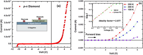
Figure 8. (a) PL of NV diamond at 300 K, and (b) time-resolved PL spectroscopy of NV diamond. The insets in (a) show SEM image and PL emission (at 532 nm excitation) of NV diamonds.
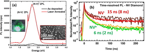
Figure 9. (a) EELS of amorphous B, intermediate superconducting layer (QB3), second superconducting phase (QB2), (b) HAADF image of B-doped Q-carbon, (c) B concentration profile, and (d) C concentration profile [Citation17].
![Figure 9. (a) EELS of amorphous B, intermediate superconducting layer (QB3), second superconducting phase (QB2), (b) HAADF image of B-doped Q-carbon, (c) B concentration profile, and (d) C concentration profile [Citation17].](/cms/asset/b2b636e9-006d-48e7-9ac6-b22d050c9257/tmrl_a_1458753_f0009_c.jpg)
Figure 10. (a) SEM image of nanodots and nanoneedles, and (b) Raman spectra of nanoneedles showing the sharp diamond peak at 1336.4 cm−1. The inset in (a) shows the characteristic Kikuchi pattern (using electron backscatter diffraction (EBSD)) of diamond.
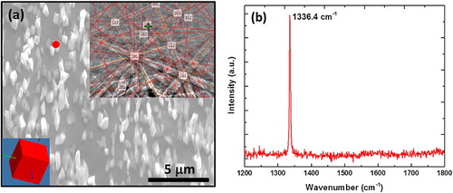
Figure 11. Field emission of Q-carbon thin film (J-E characteristics). The turn-on field (ETO) required to draw an emission current density of 30 µA/cm2 is found to be 2.65 V/µm. This field emission follows the Fowler–Nordheim model.
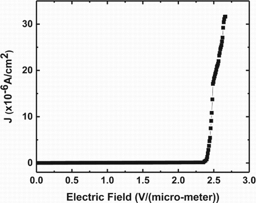
Figure 12. (a) Formation of c-BN from Q-BN, (b) large microcrystals of phase-pure c-BN, (c) microcrystals of c-BN, and (d) large-area epitaxial single-crystal films.