Figures & data
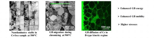
Figure 1. (a) Cross-sectional SEM image of the SMRT sample, with a magnified view of the boxed region shown by the inset. Cross-sectional (b) bright- and (c) dark-field TEM images of the near-surface layer. The inset in (b) shows the corresponding selected-area electron diffraction pattern. The dashed line in (a) marks the SMRT surface.
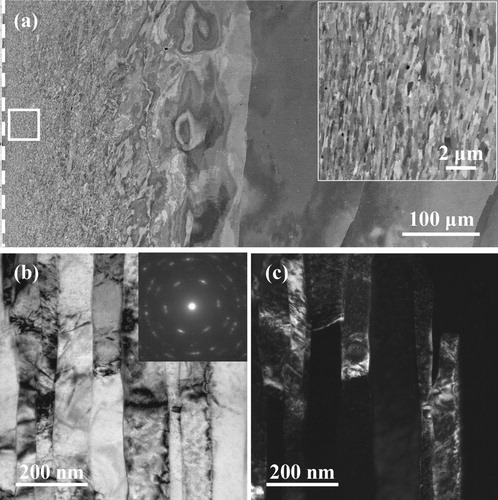
Figure 2. Cross-sectional TEM morphologies of the near-surface layers of (a) the Cr-free and (b) chromized SMRT samples treated at 500°C for 720 min. The SMRT surface is at the left side in both images. Arrows in (a) mark triple junctions (Y-junctions).
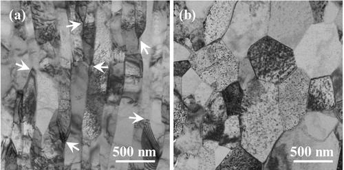
Figure 3. Cross-sectional (a) HAADF-STEM image and (b) EDS Cr mapping in the surface layer of the SMRT sample chromized at 500°C for 720 min. (c) shows the Cr profiles across 3 different GBs as marked in (a), with corresponding zero positions indicated by green dashed lines.
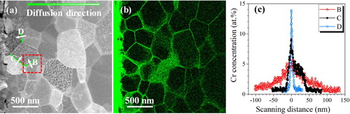
Figure 4. (a) A cross-sectional TEM morphology of the near-surface layer in the SMRT sample chromized at 500°C for 180 min. (b) HAADF-STEM image and (c) EDS Cr mapping of the boxed region in (a).
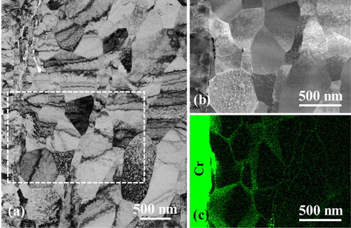
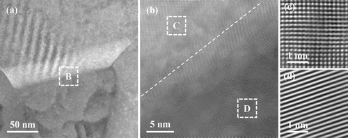
Figure 5. (a) HAADF-STEM image, (b) HRSTEM image and (c,d) magnified views (Fourier-filtered images) of the boxed regions in (b). The position of (a) is marked by a red dashed box in (a).