Figures & data
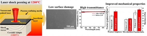
Figure 1. Schematic diagram of the high-temperature laser shock peening (HTLSP) of ceramic samples.
Figure 2. SEM images of the surface morphology of the sapphire sample (a) before LSP; (b, b’) after LSP at room temperature, which has significant surface damage; (c, c’) after HTLSP at 1200°C, which remained intact with occasional microcracks; (d) transmittance before and after HTLSP.
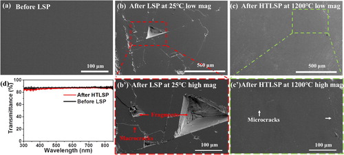
Figure 3. (a) Raman peak shift in the center of the HTLSP-treated spot. (b) Residual stress distribution in a laser-irradiated spot of the sapphire sample after HTLSP at 1200°C. (c) Scanning line of Raman spectroscopy on the surface of the laser-irradiated spot.
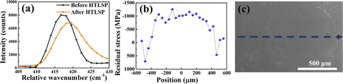
Figure 4. Diffraction-contract bright-field TEM images of cross-sectional microstructures of sapphire: (a) before HTLSP; (b, c) dislocations structures after HTLSP at 1200°C (b) near the surface and (c) at a depth of 10 µm; (d) dislocation density distribution along the depth after HTLSP at 1200°C. TEM images were taken close to the [1 1 -2 0] zone axis to reveal dislocations (marked by white arrows).
![Figure 4. Diffraction-contract bright-field TEM images of cross-sectional microstructures of sapphire: (a) before HTLSP; (b, c) dislocations structures after HTLSP at 1200°C (b) near the surface and (c) at a depth of 10 µm; (d) dislocation density distribution along the depth after HTLSP at 1200°C. TEM images were taken close to the [1 1 -2 0] zone axis to reveal dislocations (marked by white arrows).](/cms/asset/dbd05f15-d2ae-4ce4-9387-b1e74129e211/tmrl_a_1862933_f0004_oc.jpg)
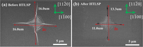
Figure 5. Comparison of the radial cracks on the edge of Vickers indentation in sapphire: (a) before HTLSP and (b) after HTLSP at 1200°C.