Figures & data
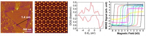
Figure 1. a, A schematic diagram of the CVD growth process. Schematic illustrations of the growth processes of Cr2Te3 using b, space-confined and c, conventional CVD, respectively. An optical microscope image of Cr2Te3 grown on mica utilizing d, the space-confined CVD and e, conventional CVD process. f, An AFM image and g, The height profile of a single Cr2Te3 flake. The thickness is ∼1.4 nm, corresponding to a single unit cell.
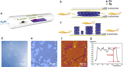
Figure 2. a, c-axis projection: unit cell of Cr2Te3 is shown in the red box; atoms with green halo are CrI atoms in the interior Cr/Vacancy layers; atoms with yellow halo are CrI atoms on the surface Cr/Vacancy layers. b, a-axis projection: braces show the structures used in calculations of single- to quad-layer. The Cr and Te columns are denoted by blue and brown solid columns, respectively. c, Atomically resolved HAADF-STEM image of single crystal Cr2Te3. Upper right inset: the reciprocal lattice obtained from an FFT of the HAADF-STEM image, with the lattice planes of Cr2Te3 highlighted by red arrows. Lower left inset: an enlarged image of c. d, EDS elemental mapping of the area shown by the red square in c. Green: Cr, Red: Te.
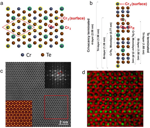
Table 1. Magnetization and MAE of 1–4 layers together with bulk Cr2Te3.
Figure 3. Competition of spin exchange, spin canting and spin-resolved total density of states (DOS). a, Schematic representation of exchange coupling in Cr2Te3. Competing inter-layer exchange parameters J12 and J13 induce canting angles for CrI and
for CrIII atoms. b,
as a function of the ratio of next-nearest to nearest neighbor exchange parameters J12/J13; the black dot represents
calculated from J12/J13 obtained using the experimental lattice constant. Spin-resolved total DOS of c, single, d, bi-, e, tri-layer and f, quad-layers Cr2Te3 calculated for Cr-terminated structures. Majority DOS is shown in the upper panels while minority DOS is shown in the lower panels. EF is the Fermi energy.
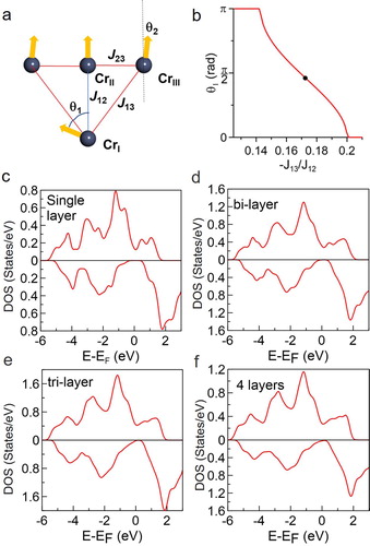
Figure 4. a, Out-of-plane magnetic hysteresis loops measured at different temperatures. b, Out-of-plane and in-plane magnetic hysteresis loops acquired at 10 K. c, ZFC and FC magnetization curves. The FC magnetization of a bulk film is also included for comparison. d, Calculated reduced magnetization as a function of reduced temperature of 2D (blue) compared to its 3D counterpart (J = 3/2, black) in the mean field approximation.
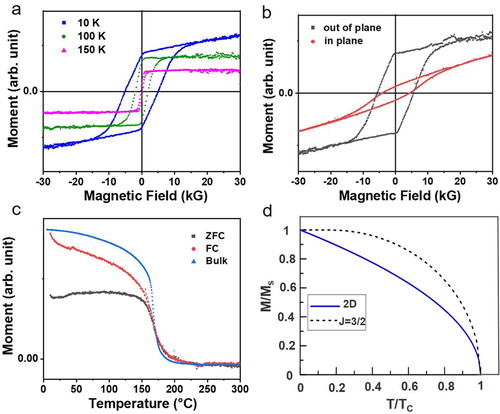
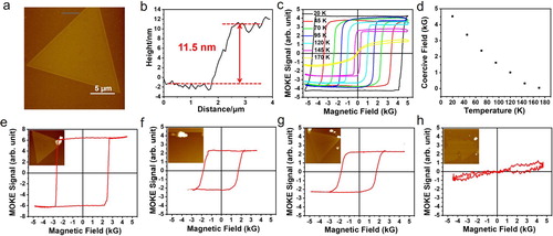
Figure 5. a, AFM image and b, the corresponding height profile of a single Cr2Te3 crystal, which shows a thickness of 11.5 nm. The black line in a corresponds to the height profile of b. c, normalized MOKE hysteresis loops and d, temperature-dependent coercivity of the corresponding Cr2Te3 crystal. e, f, g, h, MOKE hysteresis loops of Cr2Te3 2D crystals with different thicknesses, 25.2, 12.2, 7.8, and 2.8 nm, respectively. e–g were measured at 120 K; h was measured at 20 K. Inset: AFM images of the corresponding Cr2Te3 crystals.