Figures & data
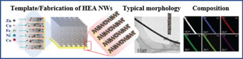
Figure 1. Schematic representation for the synthesis of 1D Co–Cu–Fe–Ni–Zn high-entropy alloy nanowires and illustration of the step-by-step process from the synthesis on AAO template to the separation of nanowires from AAO.
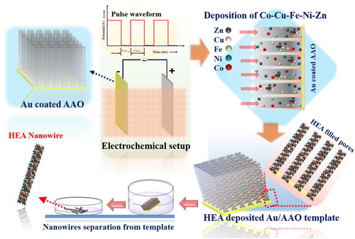
Figure 2. FEGSEM micrographs of pulse electrodeposited nanowires separated from Au/AAO template (a) aligned HEA NWs show their uniform length and flexibility (b–c) are the magnified micrographs indicating the uniform distribution in the width of the nanowires prepared by pulse electrodeposition.
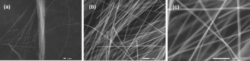
Table 1. Stoichiometry of HEA nanowire throughout the length.
Figure 3. TEM characterization of nanowires. (a) Low magnification TEM image showing the morphology and average diameter of 100 nm for a wire. (b) Bright field TEM and corresponding SAED pattern display that the nanowire is polycrystalline with FCC structure. (c) High-resolution TEM image taken on the [011] zone axis reveals that the nanowire is composed of nanotwin lamellae with spacing in the range of 1–5 nm on {111} planes.
![Figure 3. TEM characterization of nanowires. (a) Low magnification TEM image showing the morphology and average diameter of 100 nm for a wire. (b) Bright field TEM and corresponding SAED pattern display that the nanowire is polycrystalline with FCC structure. (c) High-resolution TEM image taken on the [011] zone axis reveals that the nanowire is composed of nanotwin lamellae with spacing in the range of 1–5 nm on {111} planes.](/cms/asset/92e8f01a-166f-462f-ad2c-e0d82e0a5ccc/tmrl_a_1896588_f0003_oc.jpg)
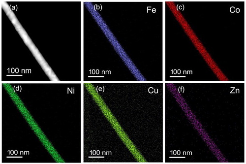
Figure 4. STEM-EDS of a nanowire. (a) HAADF-STEM image contrast shows the nanowire is polycrystalline with a grain size of few tens of nanometre in size with random orientation. (b–f) EDS chemical mapping obtained from the region reveals (b) iron (Fe), (c) cobalt (Co), (d) nickel (Ni), (e) copper (Cu) and (f) zinc (Zn), which are uniformly distributed throughout the individual nanowire.