
Figures & data
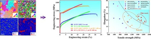
Figure 1. (a) DSC heating and cooling curves, (b) XRD patterns of as-cast (1#) and homogenized (2#) Al025 HEAs; (c)–(f) grain orientation map, EDS maps, phase distribution map and bright-field (BF) image with selected area electron diffraction (SAED) pattern of 1# Al025 HEA; (g)–(l) grain orientation map, EDS maps, phase distribution map and BF image with SAED pattern, dark-field (DF) image corresponding to superlattice spot (100) of L12 phase, BF image and SAED pattern along B2 phase [001] zone axis of 2# Al025 HEA.
![Figure 1. (a) DSC heating and cooling curves, (b) XRD patterns of as-cast (1#) and homogenized (2#) Al025 HEAs; (c)–(f) grain orientation map, EDS maps, phase distribution map and bright-field (BF) image with selected area electron diffraction (SAED) pattern of 1# Al025 HEA; (g)–(l) grain orientation map, EDS maps, phase distribution map and BF image with SAED pattern, dark-field (DF) image corresponding to superlattice spot (100) of L12 phase, BF image and SAED pattern along B2 phase [001] zone axis of 2# Al025 HEA.](/cms/asset/de1cb628-3b49-4522-aa18-d45ad34f7abd/tmrl_a_2093140_f0001_oc.jpg)
Table 1. Chemical composition (at. %) of these HEAs as determined by SEM/TEM-EDS analysis.
Figure 2. (a) SXRD patterns of recrystallized (3#) and annealed states (4#) Al025 HEAs; (b)–(d) grain orientation map, phase distribution map and EDS maps of Al025 HEA recrystallized at 900°C for 1.5 h (3#); (e) Euler distribution map and phase distribution map of Al025 HEA recrystallized at 800°C for 10 h; (f) BF image with SAED pattern of 3# Al025 HEA; (g)–(l) BF image. DF image corresponding to (100) of L12 phase with SAED pattern along L12 [001] zone axis, TEM-EDS maps of L12 region, BF image with SAED pattern along B2 [001] zone axis, TEM-EDS maps of B2 region and EDS composition profiles across B2 phase of 4# Al025 HEA.
![Figure 2. (a) SXRD patterns of recrystallized (3#) and annealed states (4#) Al025 HEAs; (b)–(d) grain orientation map, phase distribution map and EDS maps of Al025 HEA recrystallized at 900°C for 1.5 h (3#); (e) Euler distribution map and phase distribution map of Al025 HEA recrystallized at 800°C for 10 h; (f) BF image with SAED pattern of 3# Al025 HEA; (g)–(l) BF image. DF image corresponding to (100) of L12 phase with SAED pattern along L12 [001] zone axis, TEM-EDS maps of L12 region, BF image with SAED pattern along B2 [001] zone axis, TEM-EDS maps of B2 region and EDS composition profiles across B2 phase of 4# Al025 HEA.](/cms/asset/1865971a-a817-455a-804d-fa68a29cb737/tmrl_a_2093140_f0002_oc.jpg)
Figure 3. (a) Tensile engineering stress–strain curves, (b) comparison of the mechanical properties of Al025 HEA with those of existing dual-phase HEAs, (c) strain-hardening rate curves, (d) SEM images of the fracture surfaces of 4# Al025 HEA.
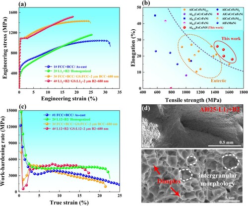
Table 2. YS, UTS, and uniform strain (US) of Al025 HEAs.
Figure 4. (a)–(c) Grain orientation map, phase map, and KAM map of 4# Al025 HEA subjected to strain of 12%; (d)–(f) BF image along L12 [011] zone axis of 4# sample; (g)–(i) Schematic of the recrystallization and deformation processes in 4# Al025 HEA.
![Figure 4. (a)–(c) Grain orientation map, phase map, and KAM map of 4# Al025 HEA subjected to strain of 12%; (d)–(f) BF image along L12 [011] zone axis of 4# sample; (g)–(i) Schematic of the recrystallization and deformation processes in 4# Al025 HEA.](/cms/asset/535b9c6c-7b8f-49b9-b1db-943334a7c476/tmrl_a_2093140_f0004_oc.jpg)