
Figures & data
Figure 1. Schematic of light scattering while traveling through isotropic polycrystalline ceramic. Adapted from Tsabit et al. [Citation13].
![Figure 1. Schematic of light scattering while traveling through isotropic polycrystalline ceramic. Adapted from Tsabit et al. [Citation13].](/cms/asset/9ddb1385-04f6-456f-bec2-ead371204d5e/tmrl_a_2109441_f0001_oc.jpg)
Table 1. Selection of thermal, optical, physical, and mechanical properties of YAG. Adapted from Kochawattana [Citation14].
Figure 2. Phase diagram for Y–Al–O system, adapted from [Citation17].
![Figure 2. Phase diagram for Y–Al–O system, adapted from [Citation17].](/cms/asset/0927e701-3e15-4df8-bcac-6b1962abcaaf/tmrl_a_2109441_f0002_oc.jpg)
Figure 3. Unit cell of YAG, adapted from [Citation19,Citation20].
![Figure 3. Unit cell of YAG, adapted from [Citation19,Citation20].](/cms/asset/8d560bfa-84d7-4ace-bce7-a8cd7d1818fe/tmrl_a_2109441_f0003_oc.jpg)
Figure 4. XRD reference patterns of YAG, YAP, YAM, B2O3, SiO2, Y2O3, and Al2O3.
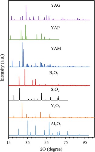
Figure 5. Fabrication rout map for co-precipitation and SSR methods.
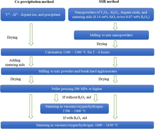
Table 2. Summary of powder synthesis and conventional sintering parameters of YAG-based polycrystalline ceramics.
Figure 6. Schematic of particle packing prior to sintering (a) and after partial sintering which has resulted in a reduced pore size (b). X is the distance between the center of the particles, this distance is reduced as sintering occurs. Replotted from L. F. Francis [Citation48].
![Figure 6. Schematic of particle packing prior to sintering (a) and after partial sintering which has resulted in a reduced pore size (b). X is the distance between the center of the particles, this distance is reduced as sintering occurs. Replotted from L. F. Francis [Citation48].](/cms/asset/624456ab-4281-4e61-a3d3-9c1c790edd31/tmrl_a_2109441_f0006_ob.jpg)
Figure 7. Change in transmittance of Yb:YAG sintered at 1750°C for 15 h as a result of ball milling time (black solid: approximate particle size; red circle: 600-nm wavelength; blue triangle: 1100-nm wavelength). Plotted based on datasets from Chen et al. [Citation57].
![Figure 7. Change in transmittance of Yb:YAG sintered at 1750°C for 15 h as a result of ball milling time (black solid: approximate particle size; red circle: 600-nm wavelength; blue triangle: 1100-nm wavelength). Plotted based on datasets from Chen et al. [Citation57].](/cms/asset/ac7cbb58-ef68-425b-9001-bed1d19f878b/tmrl_a_2109441_f0007_oc.jpg)
Figure 8. Effect of powder crystallinity on transmittance of Nd:YAG samples sintered at 1780°C for 10 h. S1–S3: calcination at 1100°C for 2, 4, 6 h, respectively. S4–S6: calcination at 1150, 1200, 1250°C respectively for 4 h. The sample S6 has the highest degree of crystallinity. Reprinted with permission from Ma et al. [Citation43].
![Figure 8. Effect of powder crystallinity on transmittance of Nd:YAG samples sintered at 1780°C for 10 h. S1–S3: calcination at 1100°C for 2, 4, 6 h, respectively. S4–S6: calcination at 1150, 1200, 1250°C respectively for 4 h. The sample S6 has the highest degree of crystallinity. Reprinted with permission from Ma et al. [Citation43].](/cms/asset/a00d47a2-a2d1-47e6-91a2-97be66c62aa2/tmrl_a_2109441_f0008_ob.jpg)
Figure 9. XRD results of powders calcinated at various temperatures. Reprinted with permission from Sang et al. [Citation28].
![Figure 9. XRD results of powders calcinated at various temperatures. Reprinted with permission from Sang et al. [Citation28].](/cms/asset/e4372e1e-5505-4857-8533-407c9d064a43/tmrl_a_2109441_f0009_oc.jpg)
Figure 10. SEM images of grain structure of sintered samples calcinated at different temperatures: (a) 900°C, (b) 1000°C, (c) 1100°C, (d) 1200°C, (e) 1300°C, (f) in-line transmittance plot of the sample shown in (e). Reprinted with permission Sang et al. [Citation28].
![Figure 10. SEM images of grain structure of sintered samples calcinated at different temperatures: (a) 900°C, (b) 1000°C, (c) 1100°C, (d) 1200°C, (e) 1300°C, (f) in-line transmittance plot of the sample shown in (e). Reprinted with permission Sang et al. [Citation28].](/cms/asset/1f45b2b1-6a50-4f32-9e3e-f2e331e864c7/tmrl_a_2109441_f0010_ob.jpg)
Figure 11. Illustration of packing structures within a green body ceramic as a result of powder morphology. Reprinted with permission from Uematsu [Citation59].
![Figure 11. Illustration of packing structures within a green body ceramic as a result of powder morphology. Reprinted with permission from Uematsu [Citation59].](/cms/asset/68e20b2c-1e38-49cc-9c30-6c08d50c0179/tmrl_a_2109441_f0011_ob.jpg)
Figure 12. Schematic of consolidation methods for producing ceramic green bodies. Replotted from Crouch et al. [Citation60].
![Figure 12. Schematic of consolidation methods for producing ceramic green bodies. Replotted from Crouch et al. [Citation60].](/cms/asset/5e3a1186-9c9f-4a79-a48a-03f28f3c88d3/tmrl_a_2109441_f0012_oc.jpg)
Figure 13. In-line transmission plot of polycrystalline 1 at. % Nd:YAG samples with the same sintering aids of SiO2 and B2O3 in flowing O2 compared to vacuum atmosphere. Reprinted with permission from Stevenson et al. [Citation22].
![Figure 13. In-line transmission plot of polycrystalline 1 at. % Nd:YAG samples with the same sintering aids of SiO2 and B2O3 in flowing O2 compared to vacuum atmosphere. Reprinted with permission from Stevenson et al. [Citation22].](/cms/asset/112764c6-4750-4ec4-82f2-7f9641704a91/tmrl_a_2109441_f0013_oc.jpg)
Figure 14. Relative density of polycrystalline YAG sintered in vacuum vs. air at given temperatures. Reprinted with permission from Mohammadi et al. [Citation27].
![Figure 14. Relative density of polycrystalline YAG sintered in vacuum vs. air at given temperatures. Reprinted with permission from Mohammadi et al. [Citation27].](/cms/asset/32d2c44d-7ac3-45b5-a73a-46fa560641d2/tmrl_a_2109441_f0014_oc.jpg)
Figure 15. Grain size increases with the increase of SiO2 concentration at given temperatures. Reprinted with permission from Stevenson [Citation81].
![Figure 15. Grain size increases with the increase of SiO2 concentration at given temperatures. Reprinted with permission from Stevenson [Citation81].](/cms/asset/022fc148-f517-4584-b3f7-8ac658a85568/tmrl_a_2109441_f0015_ob.jpg)
Figure 16. SEM images of mirror polished (top) and fractured (bottom) polycrystalline YAG with sintering aids of (A) 0.14 wt. % SiO2, (B) 0.145 wt. % SiO2 + 0.10 wt. % MgO, and (C) 0.10 wt. % MgO. Reprinted with permission from Yang et al. [Citation30].
![Figure 16. SEM images of mirror polished (top) and fractured (bottom) polycrystalline YAG with sintering aids of (A) 0.14 wt. % SiO2, (B) 0.145 wt. % SiO2 + 0.10 wt. % MgO, and (C) 0.10 wt. % MgO. Reprinted with permission from Yang et al. [Citation30].](/cms/asset/32a80751-c505-47ec-85cf-e1f0696a0fec/tmrl_a_2109441_f0016_ob.jpg)