Figures & data
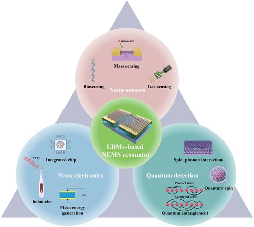
Figure 1. LDMs-based NEMS resonators in this review. The availability of diverse LDMs enabled NEMS resonators in sensings, electronics and quantum detection applications. Fundamentally, the working mechanisms, actuation and detection of representative LDMs-based NEMS resonators are included in succession.
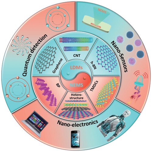
Figure 2. Prevalent fabrication routines of NEMS resonators. (a) Patterning after transfer methods [Citation47]. Take wet chemical etching technique as an example. Firstly, 2D crystal was peeled onto a sacrificial membrane (1), and then covered by a resistive mask with desired patterns (2). Later, the film was etched away by chemical solution (3), followed by removing the resist mask to obtain suspended structure (4). (b) Patterning before transfer methods [Citation50]. Take an all-dry transfer technique using PDMS stamps for example. 2D crystal was first exfoliated onto a PDMS stamp and then transferred to a pre-patterned substrate with precise alignment (1). After gently pressing (2) and peeling-off the PDMS stamp with care (3), the 2D crystal was released to form suspended micro-drumheads (4). For better understanding and demonstrative purpose, suspended 2D films in well-defined regular geometry are selected here as the working materials.
![Figure 2. Prevalent fabrication routines of NEMS resonators. (a) Patterning after transfer methods [Citation47]. Take wet chemical etching technique as an example. Firstly, 2D crystal was peeled onto a sacrificial membrane (1), and then covered by a resistive mask with desired patterns (2). Later, the film was etched away by chemical solution (3), followed by removing the resist mask to obtain suspended structure (4). (b) Patterning before transfer methods [Citation50]. Take an all-dry transfer technique using PDMS stamps for example. 2D crystal was first exfoliated onto a PDMS stamp and then transferred to a pre-patterned substrate with precise alignment (1). After gently pressing (2) and peeling-off the PDMS stamp with care (3), the 2D crystal was released to form suspended micro-drumheads (4). For better understanding and demonstrative purpose, suspended 2D films in well-defined regular geometry are selected here as the working materials.](/cms/asset/f29d2622-bfba-468b-9f4a-41825d3d3f1b/tmrl_a_2111233_f0002_oc.jpg)
Figure 3. Potential couplings between mechanical, optical, electrical, magnetic, thermal and acoustics degrees of freedom in NEMS resonators.
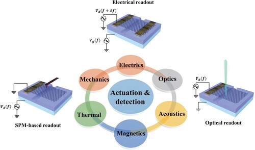
Table 1. Resonance frequency (f0), effective mass (Meff) and quality factor (Q) for reported MEMS resonators and LDMs-based NEMS resonators (G for graphene).
Figure 4. Crystal structures of representative LDMs overviewed in this work, covering CNTs, graphene, h-BN, BP, TMDCs and their heterostructures.
Table 2. Mechanical and electrical properties of several low-dimensional materials.
Figure 5. Representative actuations and detections of doubly-clamped CNTs resonators. (a) A false-color SEM image of a suspended device (top) and corresponding schematic (bottom). (b) The experimental setup. (c) Color plots of current response vs Vg and driving frequency [Citation105]. The inset shows the extracted peak positions in the frequency-gate voltage map. (d, e) SEM image and schematic of a CNTs resonator device. (f) Topography (i) and bending-mode nanotube vibration (ii-iv) images at different actuation frequencies. Zero (ii), one (iii), and two (iv) nodes correspond to first, second and third-order bending eigenmodes, respectively [Citation108] (g) Schematic of CNTs vibration measurement using an RLC resonator and a low-temperature HEMT amplifier. (h) The fundamental eigenmode displacement noise spectrum of CNTs resonators [Citation109].
![Figure 5. Representative actuations and detections of doubly-clamped CNTs resonators. (a) A false-color SEM image of a suspended device (top) and corresponding schematic (bottom). (b) The experimental setup. (c) Color plots of current response vs Vg and driving frequency [Citation105]. The inset shows the extracted peak positions in the frequency-gate voltage map. (d, e) SEM image and schematic of a CNTs resonator device. (f) Topography (i) and bending-mode nanotube vibration (ii-iv) images at different actuation frequencies. Zero (ii), one (iii), and two (iv) nodes correspond to first, second and third-order bending eigenmodes, respectively [Citation108] (g) Schematic of CNTs vibration measurement using an RLC resonator and a low-temperature HEMT amplifier. (h) The fundamental eigenmode displacement noise spectrum of CNTs resonators [Citation109].](/cms/asset/b67cbc82-5e68-4992-9d57-279df725d5e5/tmrl_a_2111233_f0005_oc.jpg)
Figure 6. Additional physics in CNTs-based resonators. (a) Schematic diagram of a CNT device (top) and relevant SEM image (bottom). (b) as function of Vsd. The yellow shaded area represents the region with self-oscillation of the device. (c) Sz vs Δω/2π curve recorded at Vsd = 0.565 mV [Citation118]. (d) Strongly-coupled CNTs resonators. Schematic diagram (left) and color mapping (middle) of the coupled resonator and double quantum dot system as a function of driving frequency and DC voltage (right) [Citation119]. (e) The acoustic resonance setup for investigating the vibration behavior of centimeter-long individual CNTs [Citation107].
![Figure 6. Additional physics in CNTs-based resonators. (a) Schematic diagram of a CNT device (top) and relevant SEM image (bottom). (b) δz2 as function of Vsd. The yellow shaded area represents the region with self-oscillation of the device. (c) Sz vs Δω/2π curve recorded at Vsd = 0.565 mV [Citation118]. (d) Strongly-coupled CNTs resonators. Schematic diagram (left) and color mapping (middle) of the coupled resonator and double quantum dot system as a function of driving frequency and DC voltage (right) [Citation119]. (e) The acoustic resonance setup for investigating the vibration behavior of centimeter-long individual CNTs [Citation107].](/cms/asset/d77e142a-9eff-41f4-9382-9557b0a3bfc0/tmrl_a_2111233_f0006_oc.jpg)
Figure 7. Graphene-based NEMS resonators manipulated by optical, acoustic and thermal approaches. (a) Experimental setup of graphene resonators by capacitive driving and optical monitoring [Citation53]. (b) 2D mapping of amplitude of reflected lights vs frequency and Vg at low laser power (300 µW) [Citation53]. (c) Log-scale amplitude vs frequency and Vg, showing the tunable frequency when graphene is self-oscillating [Citation53]. (d) A false-color SEM image of graphene-based resonator. (e) Schematic diagram of actuation and detection for graphene resonators. Ultrasonic waves propagate through the substrate to gold contacts and actuate the graphene resonator, thereby generating an electrical signal [Citation125]. (f) False-color SEM image of graphene device. Graphene sheet (blue) is suspended from the AuPd (yellow) heater and supported by surrounding AuPd islands. (g) The measured resistances as functions of heating voltages. (h) Frequency versus quality factor plot at different heating voltages [Citation126].
![Figure 7. Graphene-based NEMS resonators manipulated by optical, acoustic and thermal approaches. (a) Experimental setup of graphene resonators by capacitive driving and optical monitoring [Citation53]. (b) 2D mapping of amplitude of reflected lights vs frequency and Vg at low laser power (300 µW) [Citation53]. (c) Log-scale amplitude vs frequency and Vg, showing the tunable frequency when graphene is self-oscillating [Citation53]. (d) A false-color SEM image of graphene-based resonator. (e) Schematic diagram of actuation and detection for graphene resonators. Ultrasonic waves propagate through the substrate to gold contacts and actuate the graphene resonator, thereby generating an electrical signal [Citation125]. (f) False-color SEM image of graphene device. Graphene sheet (blue) is suspended from the AuPd (yellow) heater and supported by surrounding AuPd islands. (g) The measured resistances as functions of heating voltages. (h) Frequency versus quality factor plot at different heating voltages [Citation126].](/cms/asset/e32fc51a-7603-42e4-a4e1-2d1debd29774/tmrl_a_2111233_f0007_oc.jpg)
Figure 8. Modifications and integrations of graphene-based NEMS resonators. (a) rGO films on pre-patterned substrates. SEM images show (i) 20 nm and (ii) 4 nm thick rGO films suspended on Si pillars beds. (iii) Optical image of 3 × 3 rGO drum arrays. (iv) AFM height image of an intact drum resonator. The suspended film is approximately 10 nm below the top SiO2 surface. (v) SEM image of a drum resonator milled with a micro-hole [Citation129]. (b) Mechanical engineering of ultrathin CMG films through chemical modifications (stiffness, strength, density, and built-in stress) [Citation130]. (c) Schematic of a graphene-SiNx hybrid resonator [Citation132]. (d) Giant nonlinear response of graphene-SiNx modes after coupling graphene and SiNx resonators. (e) Coherent frequency combs of new frequency components arisen from both graphene and SiNx hybrid modes above the threshold of pump voltage. (f) Illustration of the photo-tuning effect in 2D NEMS resonators [Citation134]. (g) Resonance spectra after partial light doping at different Veff. The amplitude changes due to different conduction and driving efficiencies.
![Figure 8. Modifications and integrations of graphene-based NEMS resonators. (a) rGO films on pre-patterned substrates. SEM images show (i) 20 nm and (ii) 4 nm thick rGO films suspended on Si pillars beds. (iii) Optical image of 3 × 3 rGO drum arrays. (iv) AFM height image of an intact drum resonator. The suspended film is approximately 10 nm below the top SiO2 surface. (v) SEM image of a drum resonator milled with a micro-hole [Citation129]. (b) Mechanical engineering of ultrathin CMG films through chemical modifications (stiffness, strength, density, and built-in stress) [Citation130]. (c) Schematic of a graphene-SiNx hybrid resonator [Citation132]. (d) Giant nonlinear response of graphene-SiNx modes after coupling graphene and SiNx resonators. (e) Coherent frequency combs of new frequency components arisen from both graphene and SiNx hybrid modes above the threshold of pump voltage. (f) Illustration of the photo-tuning effect in 2D NEMS resonators [Citation134]. (g) Resonance spectra after partial light doping at different Veff. The amplitude changes due to different conduction and driving efficiencies.](/cms/asset/0f68dff5-f6b6-4233-8bb1-4dca887c3e40/tmrl_a_2111233_f0008_oc.jpg)
Figure 9. Representative NEMS resonators based on distinct TMDCs. (a) Experimental setup of monolayer WSe2 NEMS resonators [Citation62]. (b) Thermo-mechanical resonance of a MoS2 mechanical resonator (solid curve) and the fit via a finite-Q harmonic resonator model (dashed curve) [Citation77]. (c) The relationship between resonance frequency, thickness and layer number of a circular resonator [Citation77]. (d) Mechanical resonance spectra of single-layer (upper panel) and nine layers (bottom panel) MoS2 resonators. For single-layer devices, higher modes appear at frequencies corresponding to circular membranes; while for the thicker resonator, the resonance spectra agree well with the mode of circular plates [Citation57]. (e, f) Comparisons of fundamental-mode resonance frequency (f0) and Q factor dispersions [Citation200]. (g, h) Gate tuning of optically- and electrically-driven resonance in a bilayer MoS2 resonator. Colored dots represent peak amplitudes (their projections onto different planes) under different Vg values [Citation70]. (i) Nonlinear resonance of a single-layer MoS2 resonator [Citation57].
![Figure 9. Representative NEMS resonators based on distinct TMDCs. (a) Experimental setup of monolayer WSe2 NEMS resonators [Citation62]. (b) Thermo-mechanical resonance of a MoS2 mechanical resonator (solid curve) and the fit via a finite-Q harmonic resonator model (dashed curve) [Citation77]. (c) The relationship between resonance frequency, thickness and layer number of a circular resonator [Citation77]. (d) Mechanical resonance spectra of single-layer (upper panel) and nine layers (bottom panel) MoS2 resonators. For single-layer devices, higher modes appear at frequencies corresponding to circular membranes; while for the thicker resonator, the resonance spectra agree well with the mode of circular plates [Citation57]. (e, f) Comparisons of fundamental-mode resonance frequency (f0) and Q factor dispersions [Citation200]. (g, h) Gate tuning of optically- and electrically-driven resonance in a bilayer MoS2 resonator. Colored dots represent peak amplitudes (their projections onto different planes) under different Vg values [Citation70]. (i) Nonlinear resonance of a single-layer MoS2 resonator [Citation57].](/cms/asset/fb2365ac-1968-4708-be82-b1f2e840cf1f/tmrl_a_2111233_f0009_oc.jpg)
Figure 10. Recent progress of BP, h-BN and heterostructure-based NEMS resonators. (a) False-color SEM image of a BP (∼ 22 nm) resonator [Citation142]. (b, c) Measurement setup and corresponding thermo-mechanical resonance of a BP NEMS resonator under electrical tuning and driving. Inserted (c) is an optical image of the device [Citation142]. (d) Calculated fres range as functions of tensions. The horizontal line indicates the measured frequency [Citation142]. (e) Thermomechanical motion spectrum of h-BN NEMS resonators. Inset: Static reflectance mapping of the working area [Citation145]. (f) Mechanical resonance frequency (fundamental mode) vs temperature plots of h-BN drums before cleaning, after oven annealing and UV ozone cleaning [Citation63]. (g) Energy decays at various Vg. The resonator driving was stopped at t = 0 s, followed by a subsequent decay of the mechanical amplitude. The plotted traces were the averaged results of 10,000 energy decay data. Inset: a schematic of device geometry [Citation150]. (h) Fundamental and higher harmonics of a MoS2/G NEMS resonator under electrical excitation [Citation157]. (i) The predicted and measured eigenmodes for the (0,1), (1,1), (2,1), and (0,2) mechanical resonances of a 2D bimorph resonator [Citation157].
![Figure 10. Recent progress of BP, h-BN and heterostructure-based NEMS resonators. (a) False-color SEM image of a BP (∼ 22 nm) resonator [Citation142]. (b, c) Measurement setup and corresponding thermo-mechanical resonance of a BP NEMS resonator under electrical tuning and driving. Inserted (c) is an optical image of the device [Citation142]. (d) Calculated fres range as functions of tensions. The horizontal line indicates the measured frequency [Citation142]. (e) Thermomechanical motion spectrum of h-BN NEMS resonators. Inset: Static reflectance mapping of the working area [Citation145]. (f) Mechanical resonance frequency (fundamental mode) vs temperature plots of h-BN drums before cleaning, after oven annealing and UV ozone cleaning [Citation63]. (g) Energy decays at various Vg. The resonator driving was stopped at t = 0 s, followed by a subsequent decay of the mechanical amplitude. The plotted traces were the averaged results of 10,000 energy decay data. Inset: a schematic of device geometry [Citation150]. (h) Fundamental and higher harmonics of a MoS2/G NEMS resonator under electrical excitation [Citation157]. (i) The predicted and measured eigenmodes for the (0,1), (1,1), (2,1), and (0,2) mechanical resonances of a 2D bimorph resonator [Citation157].](/cms/asset/ce56d341-30de-402b-90fa-66433636aab8/tmrl_a_2111233_f0010_oc.jpg)
Figure 11. Application gallery of LDMs-based NEMS resonators.