Figures & data

Figure 1. Surface morphology characterization. The optical (a, c) and back scattered SEM (b, d) images of the non-doped (a-b) and nitrogen-doped (c-d) samples.
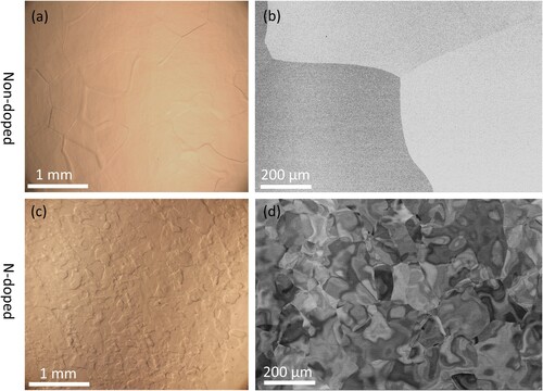
Figure 2. EBSD analysis of local misorientation. (a-c) non-doped sample and (d-f) N-doped sample. The blue squares in (a) and (d) indicate the ∼ 250 µm × 250 µm region within a coarse grain for EBSD scanning; IPF map of (b) non-doped and (e) N-doped samples, the domains with different colors in (e) represent regions with different orientations; (c) and (f) the corresponding KAM mapping of (b) and (e).
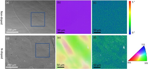
Figure 3. Microstructural and chemical analysis at Nb surface of the non-doped sample. (a) HRTEM image taken along [001] zone axis (ZA). (b) High-resolution BF-STEM image (top right inset is the corresponding fast Fourier transformation (FFT) image) shows the NbOx/Nb interface area. The white and red arrows indicate the 100 and 110 facets. The inset at the bottom right shows Nb lattice distortion close to the NbOx/Nb interface (indicated by light blue arrow). (c) schematic of Nb crystal structure with interstitial oxygen at the octahedral center, viewed along [001] ZA; (d) ABF image near the NbOx/Nb interface. The oxygen interstitials are indicated by blue arrows. (e-g) EELS analysis of the NbOx layer: (e) HAADF-STEM image and the first derivative of EELS line scan (color inset) of the Nb-M3 and O-K edges; (f-g) EELS spectrum of Nb-M2, 3 and O-K edges from positions 1–4 in (e).
![Figure 3. Microstructural and chemical analysis at Nb surface of the non-doped sample. (a) HRTEM image taken along [001] zone axis (ZA). (b) High-resolution BF-STEM image (top right inset is the corresponding fast Fourier transformation (FFT) image) shows the NbOx/Nb interface area. The white and red arrows indicate the 100 and 110 facets. The inset at the bottom right shows Nb lattice distortion close to the NbOx/Nb interface (indicated by light blue arrow). (c) schematic of Nb crystal structure with interstitial oxygen at the octahedral center, viewed along [001] ZA; (d) ABF image near the NbOx/Nb interface. The oxygen interstitials are indicated by blue arrows. (e-g) EELS analysis of the NbOx layer: (e) HAADF-STEM image and the first derivative of EELS line scan (color inset) of the Nb-M3 and O-K edges; (f-g) EELS spectrum of Nb-M2, 3 and O-K edges from positions 1–4 in (e).](/cms/asset/e8d1cca5-2891-46f2-80a2-aa55bce5d6e7/tmrl_a_2126737_f0003_oc.jpg)
Figure 4. Microstructural and chemical analysis at Nb surface of N-doped sample. (a) HRTEM image taken along [001] ZA. (b) High-resolution HAADF-STEM image shows the NbOx/Nb interface area (top right inset is the corresponding FFT), red and white arrows indicate the 110 and 100 facets. (c-e) EELS analysis of the NbOx layer: (c) HAADF-STEM image and the first derivative of EELS line scan (color inset) of the Nb-M3 and O-K edges; (d-e) EELS spectrum of Nb-M2, 3 and O-K edges from position 1–4 in (c).
![Figure 4. Microstructural and chemical analysis at Nb surface of N-doped sample. (a) HRTEM image taken along [001] ZA. (b) High-resolution HAADF-STEM image shows the NbOx/Nb interface area (top right inset is the corresponding FFT), red and white arrows indicate the 110 and 100 facets. (c-e) EELS analysis of the NbOx layer: (c) HAADF-STEM image and the first derivative of EELS line scan (color inset) of the Nb-M3 and O-K edges; (d-e) EELS spectrum of Nb-M2, 3 and O-K edges from position 1–4 in (c).](/cms/asset/b372a6cc-e1d9-4505-b9b2-22151616eebd/tmrl_a_2126737_f0004_oc.jpg)
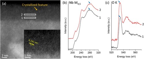
Figure 5. Crystallized feature in NbOx amorphous layer. (a) HRSTEM image shows a crystalized feature in the amorphous layer, amplifying in the inset. (b-c) the EELS data from regions 1 and 2.