Figures & data
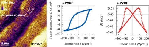
Figure 1. Surface morphology of PVDF at the micro-, nanometre and sub-nanometre scale. (a) AFM height image performed at a scan range of 50 µm, which shows the spherulites characterizing the PVDF microstructure. (b) High-resolution AFM height image showing chains organization within a spherulite at the sub-nanometre scale. (c) Schematic illustration of the spherulites structure.
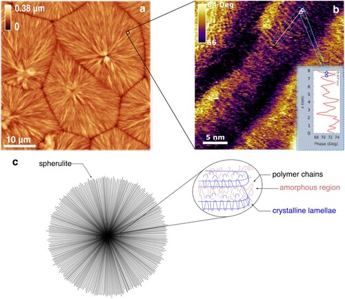
Figure 2. Chain conformation and crystal structure of P(VDF-TrFE). (a) FTIR spectrum (absorbance) and (b) XRD pattern, fitted by a Split Pearson VII, of solution-processed PVDF.
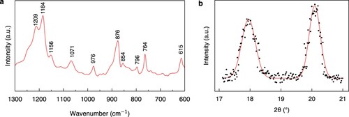
Figure 3. D-E (blue) and S-E (red) characteristics as a function of the maximum electric field applied. By increasing the electric field, we have a transformation α- to δ-phase, therefore, from a paraelectric to a ferroelectric behaviour (hysteresis loop).
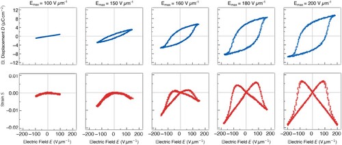
Figure 4. Polarization and ferroelectric characteristics of δ-PVDF. (a) Fit according to the Miller model (grey line) for the measured D-E data (blue circles). (b) Fit according to the electrostrictive model (grey line) for the measured electro-mechanical response (red circles).
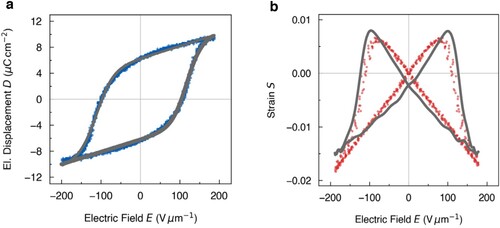
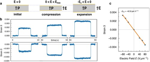
Figure 5. DC step voltage measurements and piezoelectric coefficient estimation. (a) Representation of the negative piezoelectric behaviour. (c) Plot of the S and E values collected from (b) in S as a function of E chart: the linear fitting gives d33.