Figures & data
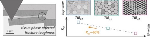
Figure 1. A FIB-manufactured TiB3.06 micro-cantilever before a micro-mechanical bending test and the post-mortem fracture cross section is depicted in a. The resulting intrinsic KIC values of TiBx coatings with x = 2.04 - 4.42 are depicted in b. In c ceramic thin film material systems are classified by their intrinsic fracture toughness (KIC) determined by micro-cantilever bending experiments and nanoindentation hardness values (H). The color-coded clouds indicate the associated material families marked in red (TM-Borides – red squares) [Citation15,Citation29], green (TM-Carbides – green circles) [Citation26–28], and blue (TM-Nitrides – blue triangles) [Citation16–25]. The obtained KIC values of TiB2 + z from this study are marked in orange.
![Figure 1. A FIB-manufactured TiB3.06 micro-cantilever before a micro-mechanical bending test and the post-mortem fracture cross section is depicted in a. The resulting intrinsic KIC values of TiBx coatings with x = 2.04 - 4.42 are depicted in b. In c ceramic thin film material systems are classified by their intrinsic fracture toughness (KIC) determined by micro-cantilever bending experiments and nanoindentation hardness values (H). The color-coded clouds indicate the associated material families marked in red (TM-Borides – red squares) [Citation15,Citation29], green (TM-Carbides – green circles) [Citation26–28], and blue (TM-Nitrides – blue triangles) [Citation16–25]. The obtained KIC values of TiB2 + z from this study are marked in orange.](/cms/asset/40995556-5c3e-4d68-85a4-5c35330b15c9/tmrl_a_2204120_f0001_oc.jpg)
Figure 2. TEM top-view analysis of the TiB3.06 coating: EF-TEM (a), STEM (b, c), and in-situ TEM-EELS was conducted (b-i, b-ii, c-ii). Section b-i depicts the electron energy loss spectrum used for the EELS line profile (white arrow in b) and indicates the B K edge at 188 eV (blue dashed line) and Ti L edge at 456 eV (green dashed line). Consequently, the resulting EELS line profile, represented in b-ii, shows detected B (blue area) and Ti (green area) – tissue phases (TP) are marked with grey areas. Section (c) shows an EELS mapping of a selected region (zoom-in in c-i). The detected elemental distribution reveals B-rich (blue) and Ti-rich (green) areas, presented in c-ii.
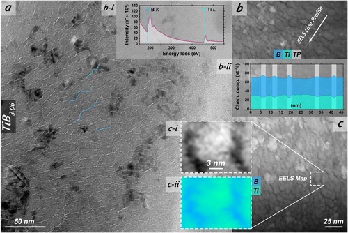
Figure 3. HR-TEM top view investigation of a TiB4.42 thin film, providing insights into inter-atomic length scales. The dashed lines in a mark certain nano-columns separated by B-rich tissue phases. A zoom-in (dashed square in a, highlights the selected area) is depicted in a-i, showing an ideally 0001 oriented column, with visible B hexagons of a basal B plane of the hexagonal TiB2 crystal lattice (SG191, P6mmm). Here, the measurements show an inter-atomic nearest B-B distance of 1.8 Å. The blue shaded area marks a ≈ 2 nm thick column-separating tissue phase (TP). In addition, b depicts a 2 × 2 × 2 AlB2 structured TiB2 supercell, with lattice constants a, b, and c. Ti and B atoms are marked in blue and green, respectively. c shows the TiB2 supercell with 0001 projection vector. B hexagons (also presented in a-i) from the B layer are visible, and B-B distances are delineated.
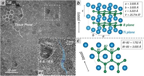
Figure 4. STEM analysis of top view prepared TiB2 + z, revealing nano-columnar morphologies of TiB2.22 (a), TiB2.43 (b), TiB3.06 (c), and TiB4.42 (d) thin films. The insets a-i, b-i, c-i and d-i represent in-situ TEM-SAED patterns in the reciprocal space of the corresponding coating. Sections e-h reveal the EELS line profiles from the marked areas (blue dashed arrows) in a-d. B is represented in blue and Ti in green, in correlation with the HAADF intensity profiles of section i-l. The sections in the EELS and HAADF spectra corresponding to the tissue phases (TP) are indicated in grey.
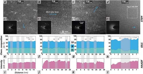
Table 1. Film stoichiometry and film thickness t, resulting from deposition pressure pdep, target-substrate distance ddep, substrate location on circular substrate holder r, deposition time tdep, and cathode tilt.
Figure A1. Characteristic pattern arising from X-Ray diffraction on the TiB2 + z highly crystalline domains. The TiB2 + z thin films on austenitic steel substrates are arranged by their B content, increasing from top to bottom (x = 2.04–4.42). For comparison, the diffraction pattern of the used TiB2/C 99/1 wt.% 6” target is plotted at the very bottom. The reference patterns for hexagonal TiB2 (SG191, P6mmm), cubic austenite (SG225, Fm-3 m), and cubic TiO (SG225, Fm-3 m) are indicated by blue squares, green triangles, and red circles, respectively.
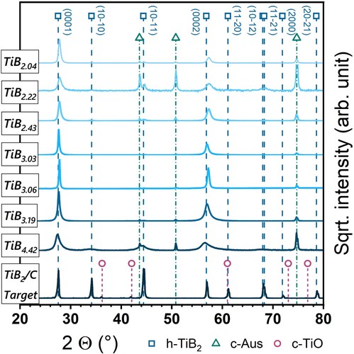
Table A1. Elemental composition from ICP-OES analysis and mechanical properties of the synthesized TiB2 + z thin films.
Figure A2. SIMS analysis of a TiB3.03 (a), TiB3.06 (b), and TiB3.19 (c) thin film. Sputtered B, Ti, and O atoms are depicted as a function of sputter time t, by blue squares, green circles, and red triangles, respectively. We acquired a depth profile in HCBU mode with a fov (field-of-view) of 100 × 100 µm at 128 × 128 px in interlaced mode, set the used sputter gun to 300 × 300 µm, and limited the measurement duration to 2000 s [1-4]. Low energy electron flooding of 21 V is used to reduce surface charging.
![Figure A2. SIMS analysis of a TiB3.03 (a), TiB3.06 (b), and TiB3.19 (c) thin film. Sputtered B, Ti, and O atoms are depicted as a function of sputter time t, by blue squares, green circles, and red triangles, respectively. We acquired a depth profile in HCBU mode with a fov (field-of-view) of 100 × 100 µm at 128 × 128 px in interlaced mode, set the used sputter gun to 300 × 300 µm, and limited the measurement duration to 2000 s [1-4]. Low energy electron flooding of 21 V is used to reduce surface charging.](/cms/asset/d8fceefa-6c48-4c76-a358-165882841746/tmrl_a_2204120_f0006_oc.jpg)
Figure A3. (a) Stress-strain data obtained by micro-pillar compression experiments of TiB3.06 thin films. The blue curves correspond to {0001} oriented TiB3.06 on sapphire substrate (b) material. σ – ϵ data from randomly oriented TiB3.06 on polycrystalline Al2O3 substrate (c) is represented by red curves. Section d depicts the XRD pattern of the TiB3.06 coating on sapphire (blue pattern) and polycrystalline Al2O3 (red pattern).
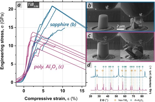
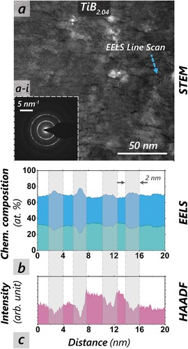
Figure A4. STEM analysis of top view prepared TiB2.04. The inset a-i represents an in-situ TEM-SAED pattern in the reciprocal space of the corresponding coating. EELS line profiles from the marked area (blue dashed arrow) in a are depicted in b. B is represented in blue and Ti in green, in correlation with the HAADF intensity profile of section c. The sections in the EELS and HAADF spectra corresponding to the tissue phases (TP) are indicated in grey.