Figures & data
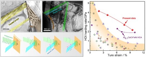
Figure 1. Microstructure of the annealed AlCoCrFeNi2 HEA before in-situ tensile deformation. (a) Phase map showing both fcc and bcc lamellae. (b1) and (b3) are inverse pole figures of bcc and fcc phases, respectively. (b2) and (b4) are size distribution of bcc and fcc phases, respectively. and
denote the average width and length of bcc phase, respectively.
denotes the average grain size of fcc phase. (c1) Bright field TEM image showing a typical interphase interface. (c2) and (c3) are selected area diffraction patterns for fcc and bcc phases. (d1) and (d2) are atomic resolution TEM images taken at the same position after tilting for α and β angles.
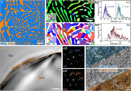
Figure 2. Dislocation activities in fcc grain interior of the AlCoCrFeNi2 HEA. (a1)–(a3) Serial in-situ TEM images from Supplementary Video 1 showing the motion of dislocations confined in a slip plane. (b1)–(b3) Screenshots from Supplementary Video 2 showing a dislocation marked by V cross-slip from a primary (11) plane onto an intersecting (1
1) plane. (c1)–(c3) Sequential snapshots of extensive cross-slip processes when two planar arrays interact with each other. See Supplementary Video 3 for further details.
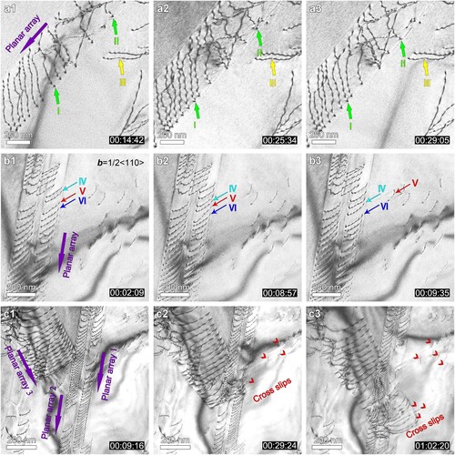
Figure 3. Interactions between dislocations and two types of boundaries in the AlCoCrFeNi2 HEA. (a1) Low magnification bright field image, showing dislocation-phase boundary interactions. (a2)–(a6) Serial snapshots from Supplementary Video 4, showing dislocations ‘reflection' by phase boundaries. (b1)–(b3) Serial snapshots from Supplementary Video 5 showing the dislocations-GB interactions.
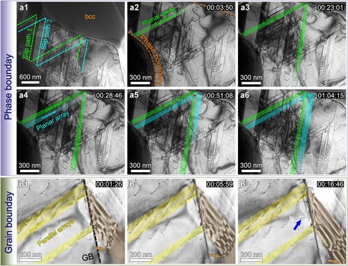
Figure 4. Mechanical properties of dual-phase AlCoCrFeNi2 HEA. (a) True stress-strain curves obtained by monotonic and loading-unloading tensile tests. (b) Enlarged unloading-reloading hysteresis loops taken from a part of a. c σHDI, σflow and σHDI/σflow against tensile strain.
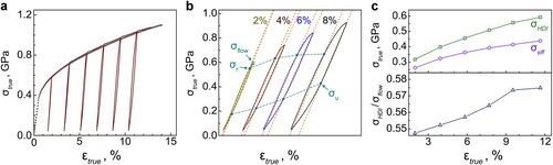
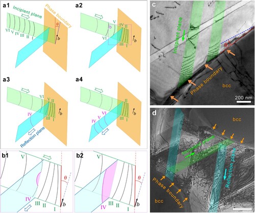
Figure 5. GND reflection mechanism at zone boundaries. (a1)–(a4) Schematic diagrams of an array of dislocations numbered as I, II, III, VI, V and VI reflecting at a zone boundary. (b1) and (b2) Close-up diagrams showing a detailed cross-slip process of GND IV. (c) and(d) Bright field TEM images showing the evidence of piling-up and reflection of GNDs at a distance from the zone boundary.