
Figures & data
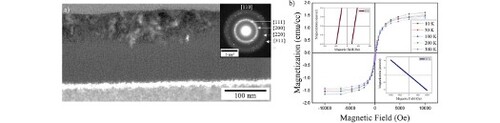
Figure 1. (a) Diamond tetrahedron D1 with central atom contained in (a/2, a/2, a/2) cube; (b) Two D1 tetrahedra connected along <110> direction; (c) Three D1 tetrahedra along <110>direction; (d) Three D1 tetrahedra: two in <110> direction (first layer) and one <1-10> direction (second layer); (e) Four D1 tetrahedra: two in <110> direction (first layer) and two <1-10> direction (second layer), this is the diamond unit cell with missing four neighboring tetrahedral; and (f) Diamond unit cell with missing four atoms from neighboring tetrahedra.
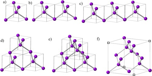
Figure 2. (a) Formation of QB3, when one central C atom is replaced by B in a three-unit (trimer) tetrahedra; (b) Formation of QB2, when one central C atom is replaced by B in a two-unit (dimer) tetrahedral; (c) Formation of QB1, when one central C atom is replaced by B in a three-unit tetrahedra (trimer); and (d) Formation of QB1, when one central C atom is replaced by B in a three-unit tetrahedra in two layers.
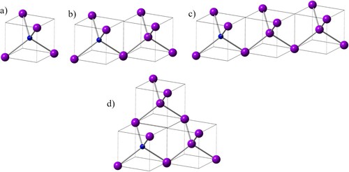
Figure 3. (a) Four D1 tetrahedra in one plane (D14); (b) Eight tetrahedra in two planes, leading to formation of Q-diamond subunit cell with net 16 atoms; and (c) Formation of Q-diamond super unit cell with four subunit cells: two in <110> direction and two in <1-10> direction (d) with missing four neighboring subunit cells, similar to missing tetrahedra in the diamond unit cell. By replacing central C atoms in these tetrahedra by B atoms selectively, 50% B-doped Q-diamond phase is created, having net 32 C and 32 B atoms arranged in two layers.
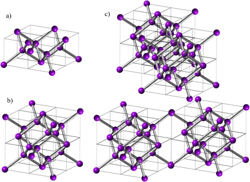
Table 1. Atom coordinates for B-doped Q-carbon subunit cell and super unit cell. Four common atomic positions between different subunit cells are indicated by C* and common between A and B subunits.
Figure 4. High-resolution TEM micrograph showing formation of Q-silicon: (a) <110> cross-section TEM with 85 ± 5 nm Q-silicon layer and inset diffraction pattern with 111, 200, 220, and 311 continuous diffraction rings; (b) Interface between Q-silicon and amorphous silicon; and (c) Nanocrystallites in Q-silicon with nanotwins. (d) EELS spectrum from crystalline (c-Si), amorphous (a-Si) and Q-silicon (Q-Si), showing Si L23 edge remains unchanged
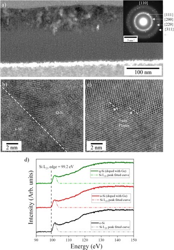
Figure 5. Raman Spectra: (a) Unannealed amorphous silicon (Ge+ implanted); (b) Laser annealed with 0.1 Jcm−2 (c) Laser annealed with 0.2 Jcm−2, (d) Laser annealed with 0.3 Jcm−2, and (e) Magnetization (M) versus field (H) at 10 K, 50 K, 100 K, 200 K and 300 K of 0.3 Jcm−2 sample with inset (top left) showing coercivity associated with ferromagnetism (intercept along the x-axis), and other inset (bottom right) showing diamagnetic behavior in as-implanted samples before laser annealing.
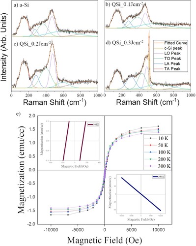
Table 2. TA, LA, LO, TO and crystalline modes in Raman spectra of Figure , before annealing and after annealing with 0.1, 0.2, and 0.3 Jcm−2.